Join us for the March Characterization User Forum focused on Electron Backscatter Diffraction (EBSD).
DATE: Wednesday, March 18, 2026
TIME: 4:00 p.m. — 5:00 p.m. ET
LOCATION: 12-0168 (MIT.nano basement teaching space)
- Get to know your Characterization community.
- Bring questions about your data.
- Share your feedback in a user-led town hall.
- Stay up-to-date with facility news.
- Food and drink will be provided.
Each user forum also includes a spotlight talk by a graduate student, postdoc, or researcher. The March forum will feature:
A brief introduction to Electron Backscatter Diffraction and MIT.nano's capabilities
Speaker
Connor Moorman
Research specialist, MIT.nano
Abstract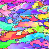 Electron Backscatter Diffraction (EBSD) offers a wealth of information with every scan. Every crystal structure in a material has a story to tell, and EBSD is one of the most scientifically rich and visually striking methods for telling that story. Whether you are interested in just verifying the orientation of a single crystal phase, producing a vivid color map of many complex grains with inverse pole figures, or exploring the stress that may have accumulated in your material due to misorientations, EBSD can do it all with just a single scan.
In this presentation, Connor will go over the background behind EBSD, how MIT.nano’s EBSD system works, what type of information you are able to collect, as well as what some of the newest EBSD methods can do.
If you want to explore the full extent of your crystalline materials while also producing some of the most visually striking images, then EBSD is here to lead the way.
Image caption: Inverse Pole Figure Map of crystal orientations in a 3D printed titanium alloy.
Biography
Connor is a research specialist at MIT.nano who manages SEM's and other metrology equipment used for the characterization of materials.