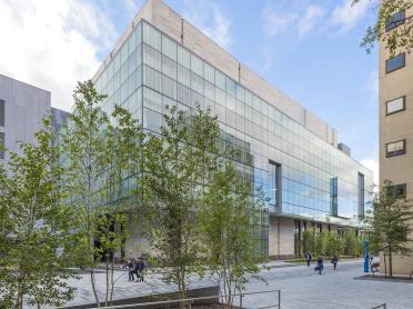
MIT.nano is MIT's central resource for nanoscale discovery and innovation, set in the heart of campus in the Lisa T. Su Building.
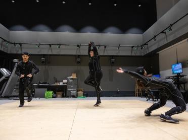
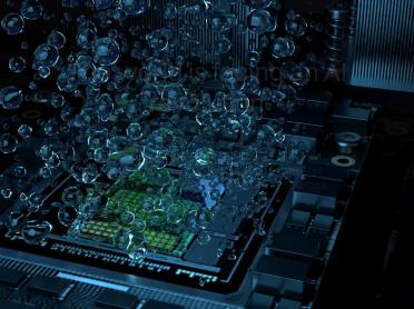
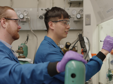
We have three main facilities: Fab.nano — more than 45,000 sq. ft. of ISO 5, 6, 7 (class 100, 1,000, 10,000) cleanroom with capabilities spanning lithography, etching, deposition, diffusion, and wet processing. Characterization.nano — 11,000 sq. ft. for metrology and characterization including 12 sophisticated suites for nanoscale observation with low vibration and minimal electromagnetic interference. The Immersion Lab — an environment to connect the physical to the digital — visualizing data, prototyping advanced tools for augmented and virtual reality (AR/VR), and developing software and hardware concepts for immersive experiences.