Archana Raja, PhD

Staff Scientist, Molecular Foundry, Lawrence Berkeley National Laboratory
Affiliate Faculty, Kavli Energy and NanoScience Institute, UC Berkeley
Date: December 2, 2024
Time: 3:00 - 4:00 PM ET
Location: Building 34, Room 401 (Grier Room)
Reception to follow
Abstract
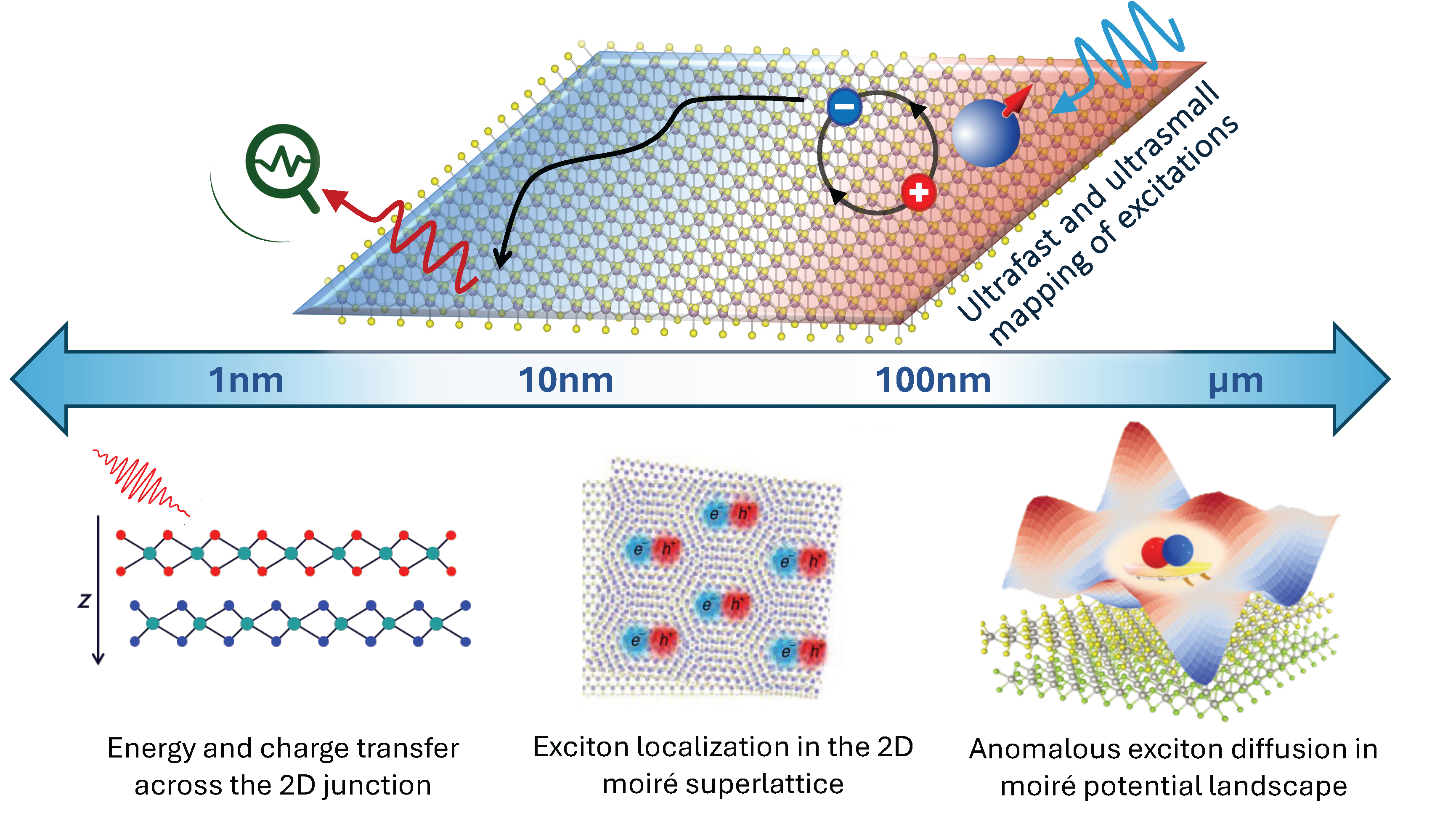
Atomically thin van der Waals crystals like graphene and transition metal dichalcogenides allow for the creation of arbitrary, atomically precise interfaces simply by stacking disparate monolayers without the constraints of covalent bonding or epitaxy. By leveraging the environmental sensitivity of interactions at the ultra-thin, two-dimensional (2D) limit, we can “paint” potential energy landscapes to create and control the electronic structure and excitations in these systems.
Raja and her colleagues have characterized and discovered phenomena in such 2D potential landscapes from the atom scale to the application scale using multimodal photon and electron-based spectroscopies.
In this talk, Raja will discuss stories from her joint experimental and theoretical work on the prototypical 2D semiconductor interface of monolayer WS2 and monolayer WSe2. In part one, the team used ultrafast electron diffraction to reveal the role of layer-hybridized electronic states for controlling energy and charge transport across atomically sharp junctions [1]. In part two, they aligned the registry of the two layers and used electron energy loss spectroscopy to directly visualize the real space localization of excitonic states within a single moiré unit cell [2], opening the possibility of engineering excitonic superlattices with nanometer precision. The third and final part focused on the transport of energy across such a superlattice potential using interlayer excitons [3]. Raja and her colleagues have uncovered unexpected trends in the temperature-dependent exciton diffusivity, which suggests that the moiré potential landscape is dynamic down to very low temperatures.

[1] A. Sood*, J. Haber*, A. Raja et al. “Bidirectional phonon emission in two-dimensional heterostructures triggered by ultrafast charge transfer,” Nature Nanotechnology 18 (1), 29-35 (2023)
[2] S. Susarla*, M. H. Naik*, A. Raja et al. “Hyperspectral imaging of excitons within a moiré unit-cell with a sub-nanometer electron probe,” Science 378 (6625), 1235-1239 (2022)
[3] A. Rossi*, J. Zipfel*, I.Maity*, A. Raja et al. “Anomalous interlayer exciton diffusion in WS2/WSe2 moiré heterostructure,” ACS Nano 18 (28), 18202-18210 (2024)
Biography
Archana Raja completed her PhD in Chemical Physics from Columbia University under the supervision of Profs. Tony Heinz and Louis Brus in 2016. After spending a year as a postdoc in the Applied Physics department at Stanford University, she joined the Kavli Energy and NanoScience Institute at UC Berkeley as a Heising-Simons fellow in Prof. Paul Alivisatos' group. In July 2019, she became a staff scientist at the Imaging and Manipulation of Nanostructures Facility at the Molecular Foundry. In 2024, she became an affiliated faculty member of the Kavli Energy and NanoScience Institute.
Raja is the recipient of the LBNL Director’s Award for Exceptional Achievement in Early Scientific Career, Early Career Lab Directed Research Development Award, Blanche R. and David Kasindorf Fellowship in Physical Chemistry at Columbia University, the Institute Silver Medal at the Indian Institute of Technology in Bombay, and was recognized as part of the 2019 Rising Stars in Physics cohort.
