Technological breakthroughs for EBSD: Faster mapping and greater sensitivity
WHERE AND WHEN
Thursday, November 12, 2020
11 am – 1 pm EST
Attendees can join via Zoom.
Meeting ID: 945 8610 0937
REGISTER
DETAILS
Presented by: Shawn Wallace, EBSD Applications Engineer, EDAX
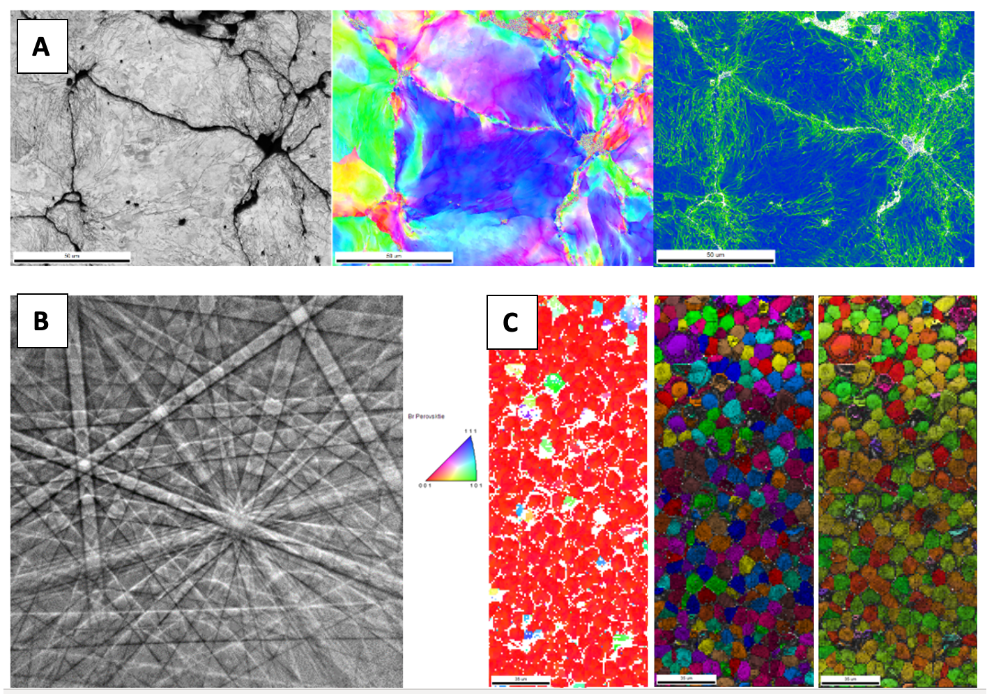
Recent advances in Electron Backscatter Diffraction (EBSD) hardware have gone two ways—speed or performance. Newer CMOS detectors have pushed speeds to unthinkable levels, allowing fine spatial resolution data sets to be taken over large areas. Performance-wise, the advent of using direct electron detection methods as an EBSD sensor has pushed the technique to newer, more beam-sensitive materials. This has allowed mapping to occur with less than 50 photon events per sensor pixel. Correlating either the large area maps collected at high speeds or the smaller more sensitive maps with other techniques can show the power of combining different material characterization methods.
This seminar will focus on showing how combining EBSD with nanoindentation can help reveal crystal orientation influence on the mechanical properties of materials. Additional application data will also show how correlating EDS data with EBSD data can be useful in some cases.