The impact of Atomic Layer Deposition in our world and Arradiance’s contribution to leading edge research
Tuesday, September 13
11AM – 12PM: Seminar in-person only; 12-0168
12PM – 1PM: Lunch break
1PM – 2PM: Group 1 Demo inside MIT.nano's cleanroom
2PM – 3PM: Group 2 Demo inside MIT.nano's cleanroom
>>Register.
Atomic layer deposition (ALD), conceptualized in the 1950s and commercialized in the late 60s and 70s, plays a critical role in nearly every aspect of our lives today. ALD is utilized in almost everything we purchase, and even plays a role in our security and space programs.
 Enabling continued miniaturization of the electronics in our world, ALD has the unique capability of depositing conformal monolayers of film over complex 3D nano structures. With the addition of Plasma Enhanced ALD, manufacturers and researchers alike have almost unlimited access to the Periodic Table, accommodating a wide variety of substrates, even with low temperature budgets. ALD can be used to modify interfacial layers, protect devices from their environment, and fabricate nanostructures with improved material and electrical properties.
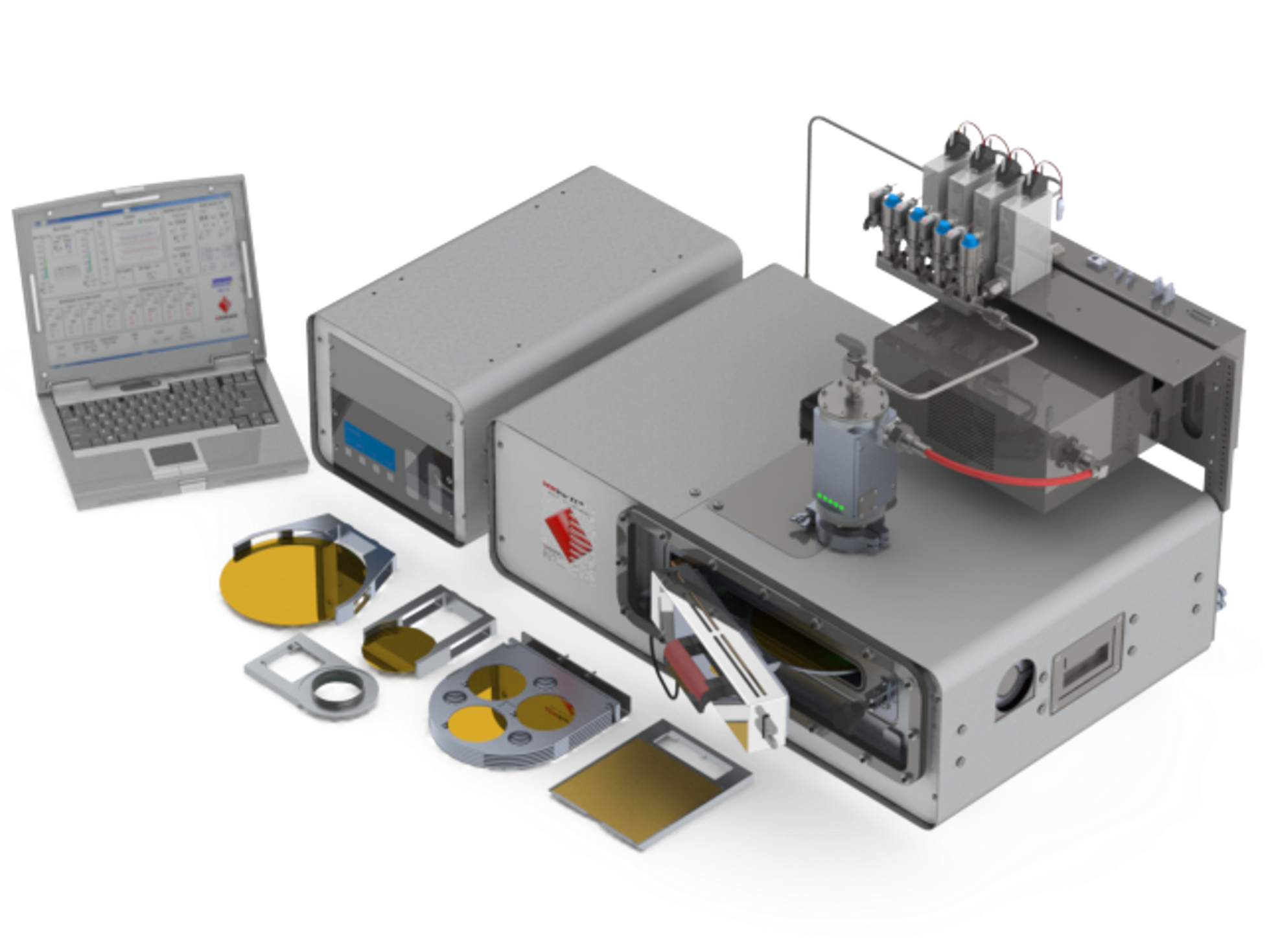
This talk will focus on the attributes of the Arradiance GEMStar PEALD System and how its unique configurability supports some of the most demanding research programs around the world and in user facilities like MIT.nano.