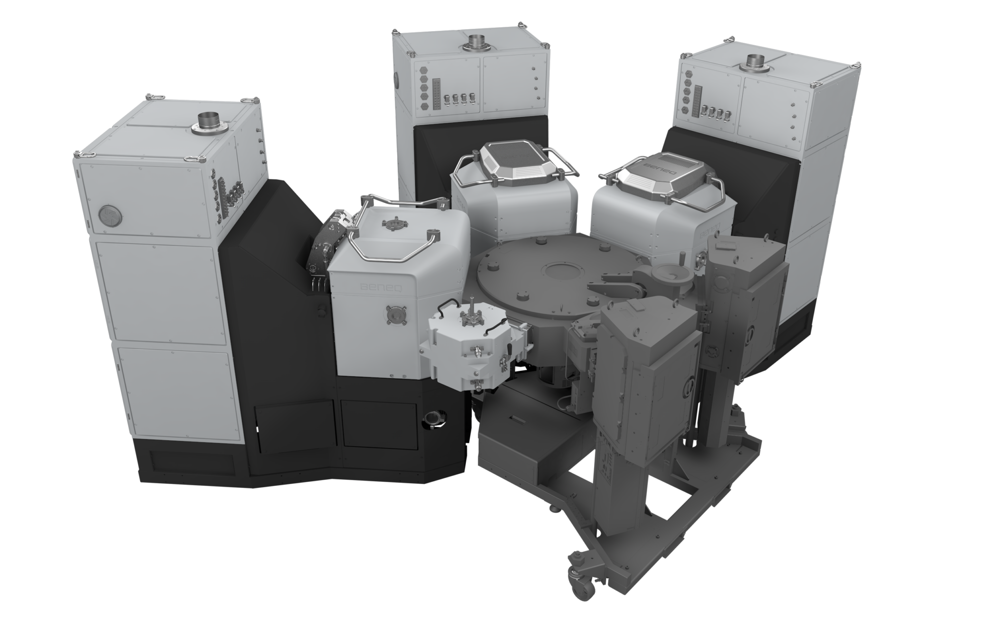
Beneq Transform—Versatile, automated ALD solution for high-throughput semiconductor production
WHERE AND WHEN
DATE: Tuesday, June 14, 2022
TIME: 10 a.m. – 11 a.m. EDT
LOCATION: Via Zoom: mit.zoom.us/j/94586100937
SPEAKER: Patrick Rabinzohn, Product Strategy and Business Development, Executive Semiconductor ALD, Beneq
Open to MIT community members.
>>REGISTER
DETAILS
With its unique capability to precisely and conformally deposit a large range of critical materials as pin-hole free thin films at low temperature, Atomic Layer Deposition (ALD) is set to enable More-than-Moore (MtM) device technologies for the years to come. The challenges for adoption of ALD in the production of MtM devices are twofold. First, MtM devices need to face technology inflections for which ALD becomes a must. Second, generally the throughput of ALD is perceived to be too low or its cost of ownership too high.
Regarding the first challenge, ALD is the way to go when surface and interface control is critical and/or films with high quality, conformality, and uniformity are needed. When it comes to throughput, one order-of-magnitude improvement is made possible by Beneq’s advanced batch thermal ALD technology. This is sometimes called mini-batch – designed for standard wafer handling systems and advanced cluster tool design, incorporating a rapid pre-heating for manufacturing worthiness. Beneq Transform and Transform 300 ALD cluster tools, as well as Beneq Prodigy standalone equipment, deliver manufacturing worthy processes with versatility for wafer sizes from 75 mm to 300 mm. Transform and Transform 300 are ALD cluster tools offering both Thermal ALD (batch) and Plasma ALD (single wafer) technologies for maximum flexibility and capability to enable various capacity, product, and application mixes.
In addition to introducing Beneq ALD technology and Transform cluster tool, this presentation will provide an overview of current and future applications of ALD across power devices, RF filters and ICs, MEMS and sensors/actuators, Image sensors, LEDs and light detectors, VCSEL, Micro-LED, photonics, Micro-OLED, and future market segments. It will emphasize the ALD materials and technologies that enable functionalities such as high-k, surface passivation, nucleation and seed, chemical and moisture barriers, anti-reflective coating. Dr. Rabinzohn will also emphasize critical applications in the market segments of compound semiconductor devices.
About Patrick Rabinzohn
Dr. Rabinzohn is an executive for the Semiconductor ALD Business Unit at Beneq, responsible for product strategy and business development. He has 40 years of semiconductor industry experience across the semiconductor, semiconductor equipment and materials markets, and has extensive knowledge on equipment, process, process integration, and technologies.
Prior to Beneq, Rabinzohn held several high-profile roles including CTO for IoT/MEMS and Advanced Packaging at Lam Research, General Manager at Intermolecular, Managing Director for Microelectronics at Alchimer, and CTO Europe at Applied Materials. He graduated from Ecole Superieure d’Electricite (Supelec) and received a Ph.D. in Materials Science from Paris University.
ABOUT BENEQ
Beneq established the world’s first industrial production using atomic layer deposition (ALD) in 1984. Today, they are a recognized provider of ALD equipment and R&D services. Beneq's mission is to create premium tools for production and for research, and to enable technology mega trends through industrial ALD solutions.