Please join us for the May MIT.nano Seminar Series:
 Rehan Kapadia
Assistant Professor, Electrical & Computer Engineering
Colleen and Roberto Padovani Early Career Chair
University of Southern California
Date: Monday, May 17, 2021
Time: 3pm - 4pm EDT
Location: Zoom webinar
To receive event announcements, sign up for our email list.
Abstract
As Moore’s Law ends, the search for approaches enabling faster computing systems and diversification of semiconductor device applications has significantly intensified. In Kapadia's group, researchers work on challenges through the lens of two questions:
- Can materials and devices be grown at low-temperatures and on non-epitaxial substrates to enable functional diversification of CMOS platforms?
- Can hot-electrons be used efficiently in electronic and optoelectronic devices?
In the first part of his talk, Kapadia will discuss his work on growing III-V semiconductors on non-epitaxial substrates using a combination of templated liquid phase growth (TLP) and metal-organic chemical vapor deposition (MOCVD). Specifically, he will discuss the fundamentals of the TLP growth technique, which enables crystalline III-V mesas to be grown directly on oxide and metal substrates. This is achieved by creating micro-scale metal templates (e.g. indium), and then carrying out a phase transformation to change each template into a single crystalline III-V (e.g. InP).
After discussing the basic growth processes and resulting material quality, Kapadia will highlight some recent results with TLP growth at CMOS back-end compatible temperatures of <400oC. Due to the low temperature used here, these material growth techniques are directly compatible with back-end CMOS integration. Uniquely, it is shown that InAs grown directly on oxides at 300oC exhibits mobilities of ~5800 cm2/V-s. He will then discuss electronic devices fabricated from TLP based materials, specifically III-V on oxide MOSFETs and synaptic devices.
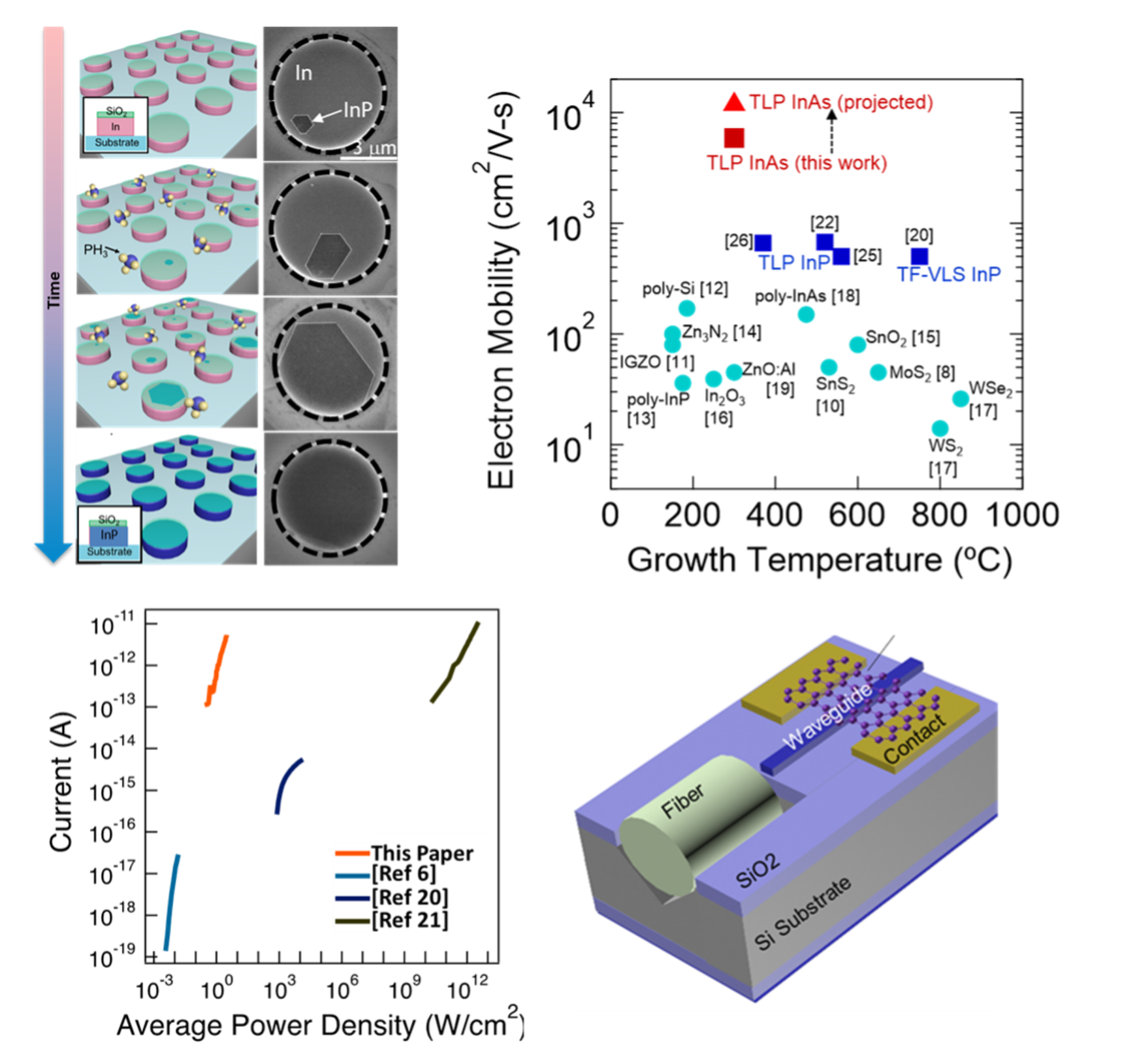
Next, Kapadia will show how hot-electron processes can dramatically reduce the optical power densities required for photoemission. Specifically, he will show that a waveguide integrated graphene electron emitter excited with 3.06 eV photons from a continuous wave (CW) laser exhibits two hot-electron processes that drive photoemission at peak powers >5 orders of magnitude lower than previously reported multi-photon and strong-field metallic photoemitters. Optical power dependent studies combined with modeling illustrate that the observed behavior can be explained by considering direct emission of excited electrons. Theoretical and simulation exploration of the fundamental limits of this process highlights that a new class of ultra-fast electron emitters could be enabled using the hot-electron emission process in conjunction with integrated photonics.
Finally, Kapadia will briefly demonstrate a hot-electron electrochemical device, where hot electrons are used to modify the reaction rates of the hydrogen evolution reaction (HER) on an electrode immersed in solution. It is observed that hot-electrons injected from silicon into a thin gold layers demonstrates quantum efficiencies of >50% when driving the hydrogen evolution reaction.
Biography
Professor Kapadia joined the faculty of the University of Southern California (USC) in the Ming Hsieh Department of Electrical and Computer Engineering in July 2014 and holds the Colleen and Roberto Padovani Early Career Chair. He received his bachelors in electrical engineering from the University of Texas at Austin in 2008, and his Ph.D. in electrical engineering from the University of California, Berkeley in 2013.
During his time at Berkeley, Kapadia was a National Science Foundation Graduate Research Fellow and winner of the David J. Sakrison Memorial Prize for outstanding research. At USC, he has been the recipient of an Air Force Young Investigator Award and the AVS Peter Mark Memorial Award. His interests lie at the intersection of material science and electrical engineering, with a focus on developing next-generation electronic and photonic devices for computing applications beyond CMOS, such as bio-inspired devices and non-von Neumann computing. Additionally, Kapadia is the co-director of a recently created Center for Integrated Electronics and Biological Organisms (CIEBOrg) at USC.