Enabling novel devices with the NanoFrazor
Date: Thursday, October 26, 2023
Location: 12-0168 (MIT.nano basement)
Speaker: Dr. Emine Çağın, CTO, Heidelberg Instruments Nano
Schedule:
11:00 AM – 12:00 PM: Seminar
12:00 PM – 1:00 PM: Lunch sponsored by Heidelberg Instruments Nano
1:00 PM – 3:00 PM: Live demo in the MIT.nano first floor cleanroom
Abstract
The NanoFrazor is a nanofabrication tool that combines thermal scanning probe lithography (t-SPL) and direct laser sublimation (DLS) to create nano and microstructures rapidly and repeatably. Advances in the technology open new application areas and enable novel research in a wide range of material systems. In t-SPL, an ultrasharp tip is heated for a few microseconds at each pixel in order to remove thermal resist materials. When used in a closed-loop system, t-SPL can be used to write grayscale structures and to control the depth of lithography to optimize post-processing. DLS employs a focused laser beam to remove the same resist materials to quickly and simply create microstructures.
The high-resolution, rapid patterning capabilities of the NanoFrazor are increasingly used in nanoelectronic circuits, including shaping MoS2 in a deterministic manner1 and creating edge-contacts to MoS2 transistor devices2. The versatility of t-SPL is exploited in applications that benefit from freeform patterning of arbitrary shapes on a large variety of materials, such as forming nanodisks, nanoparticles, and even nanoflowers in a reproducibly3. The arbitrary patterning capability is combined with grayscale patterning to create varied-thickness flakes of hexagonal boron nitride for future nanoelectronics applications4. Furthermore, advances in processing with more resist materials, including polymers such as parylene C5, add to the flexibility of the technique.
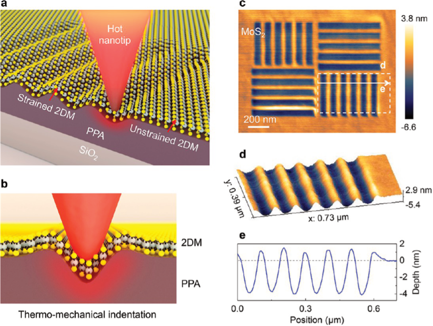
In this seminar, current and future applications and capabilities with the NanoFrazor will be explored. Applications beyond nanolithography, such as thermomechanical nanostraining6, direct control of spin orientations, and triggering of reduction reactions will be highlighted. Emerging materials and novel device concepts enabled with the tool will also be discussed.
1 M.C. Giordano, et.al., Adv. Mat. Interfaces, 2201408 (2022).
2 A.Conde-Rubio, et.al., ACS Appl. Mater. Interfaces, 14, 37 (2022).
3 T. Das, et.al., ACS Appl. Mater. Interfaces 14, 17 (2022).
4 N. Lassaline, et.al., Nano Letters, 21, 19 (2022).
5 Y. Jiang, et.al, Micro & Nano Lett. 17, 4 (2022)
6 X. Liu, et.al., Nano Letters, 20, 11 (2020)