Atomic Layer Etching (ALE) and the Bosch Process
DATE: Friday, June 27, 2025
TIME: 11 a.m. – 1 p.m.
LOCATION: MIT.nano (12-0168)
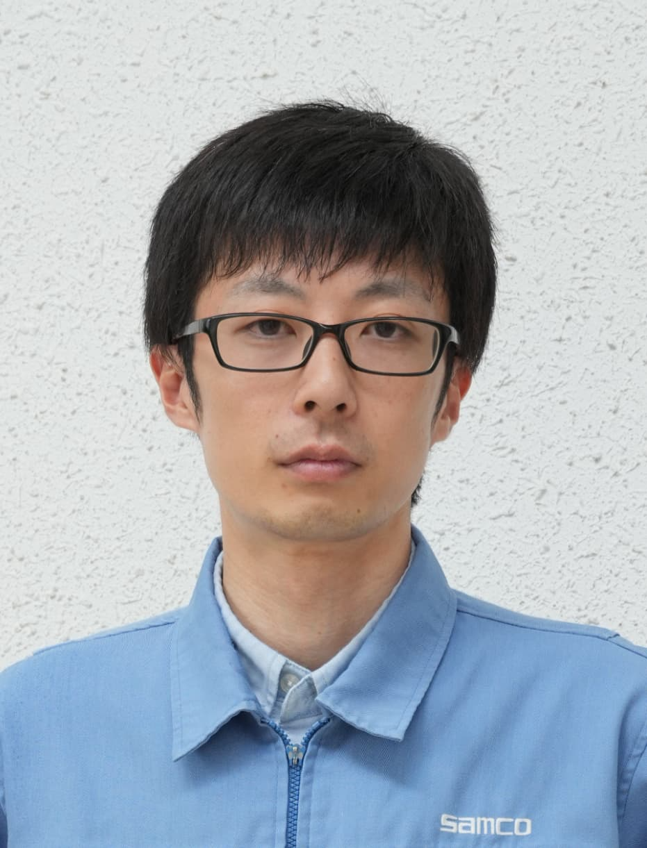
SPEAKER: Akimi Uchida, Lead Engineer, R&D Department, Samco Inc.
Register for this presentation
Abstract
Atomic Layer Etching (ALE)
Atomic Layer Etching (ALE) is an advanced plasma-based technique that enables highly precise and selective removal of materials at the atomic scale—an essential capability in cutting-edge semiconductor manufacturing. ALE achieves this by alternating between surface modification and material removal steps, allowing for precise control that traditional continuous etching methods cannot offer.
The process typically involves chemically activating the surface through adsorption, followed by the selective removal of that activated layer using plasma or low-energy ion irradiation. These reactions are self-limiting, meaning the etching naturally halts at a single atomic layer. This results in exceptional selectivity and uniformity, making ALE especially valuable for sub-10 nm device fabrication, 2D materials, high-aspect-ratio structures, and complex 3D integration.
Bosch Process
The Bosch Process, developed by Robert Bosch GmbH in 1992, is a deep silicon etching method that enables the formation of high-aspect-ratio features with near-vertical sidewalls. Samco became the first Japanese manufacturer to obtain a license for this process in 2003.
The technique alternates between two steps: an isotropic etching step (typically using sulfur hexafluoride, SF₆) and a passivation step (using gases like C₄F₈ to deposit a protective polymer on sidewalls). By repeating this cycle, the process achieves highly directional etching with excellent precision and productivity. It is widely used in applications such as MEMS devices and through-silicon vias (TSVs).
With extensive expertise in plasma-based technologies for etching, deposition, and cleaning, Samco continues to advance both ALE and Bosch process capabilities. This presentation will introduce recent developments in these areas, including process data and system innovations.
Speaker Bio
Akimi Uchida is a lead engineer in the R&D Department at Samco Inc., originally from Mihara City in Hiroshima Prefecture. He received his bachelor's degree in Electrical and Electronic Engineering from Yamaguchi University in 2010, followed by a master's degree in Science and Engineering in 2012. Since joining Samco the same year, he has played a central role in the development of atomic layer etching (ALE) and Bosch process etching systems. His work focuses on advancing precision etching solutions to support next-generation semiconductor fabrication. In recognition of his outstanding contributions to equipment innovation and the expansion of Bosch system sales, he received a company award for excellence.