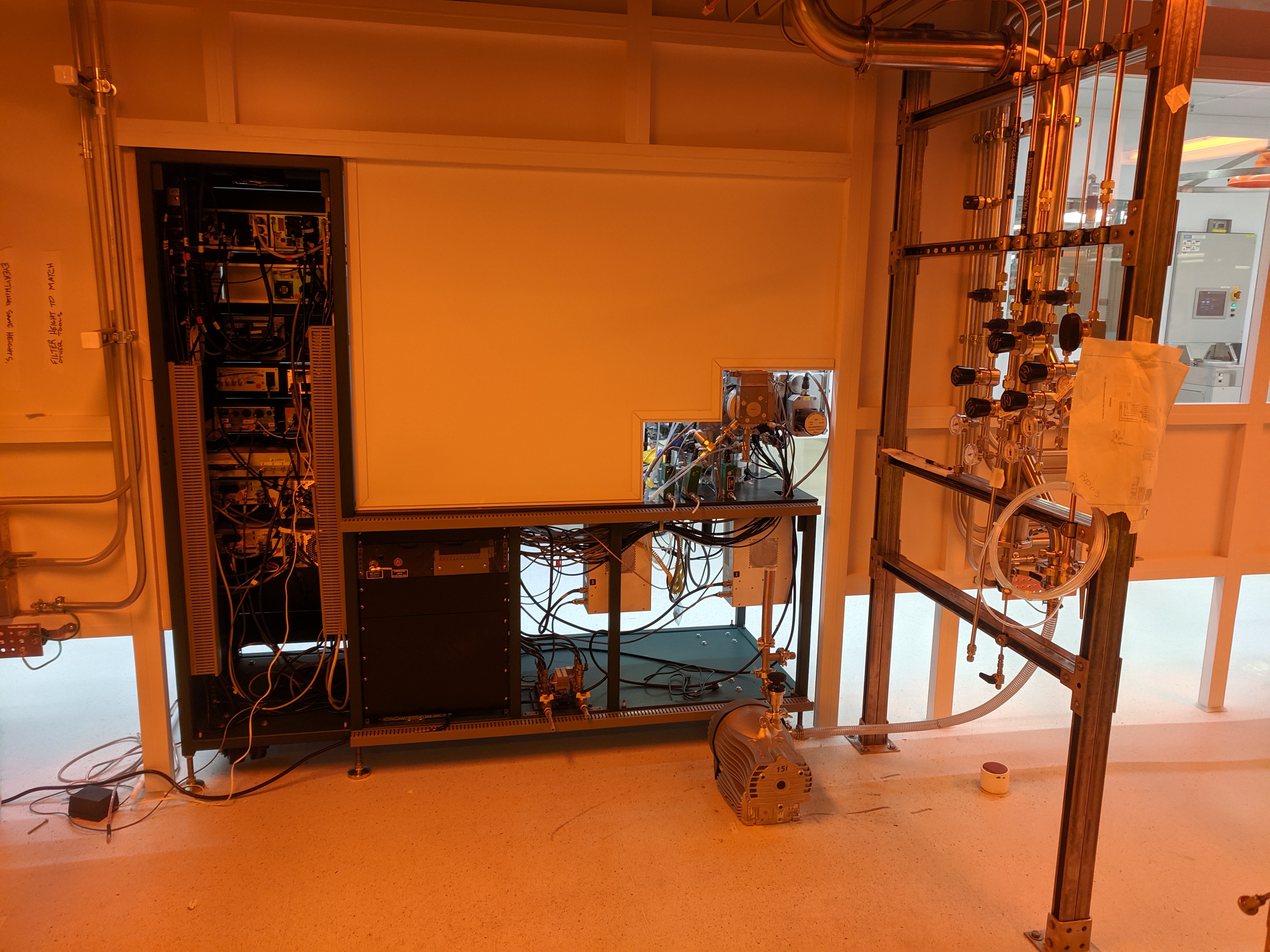
After moving the AJA sputter system to MIT.nano last week, installation is ongoing. Most of the action is behind the scenes in the chase where pumps and other utilities are now being placed and connected.
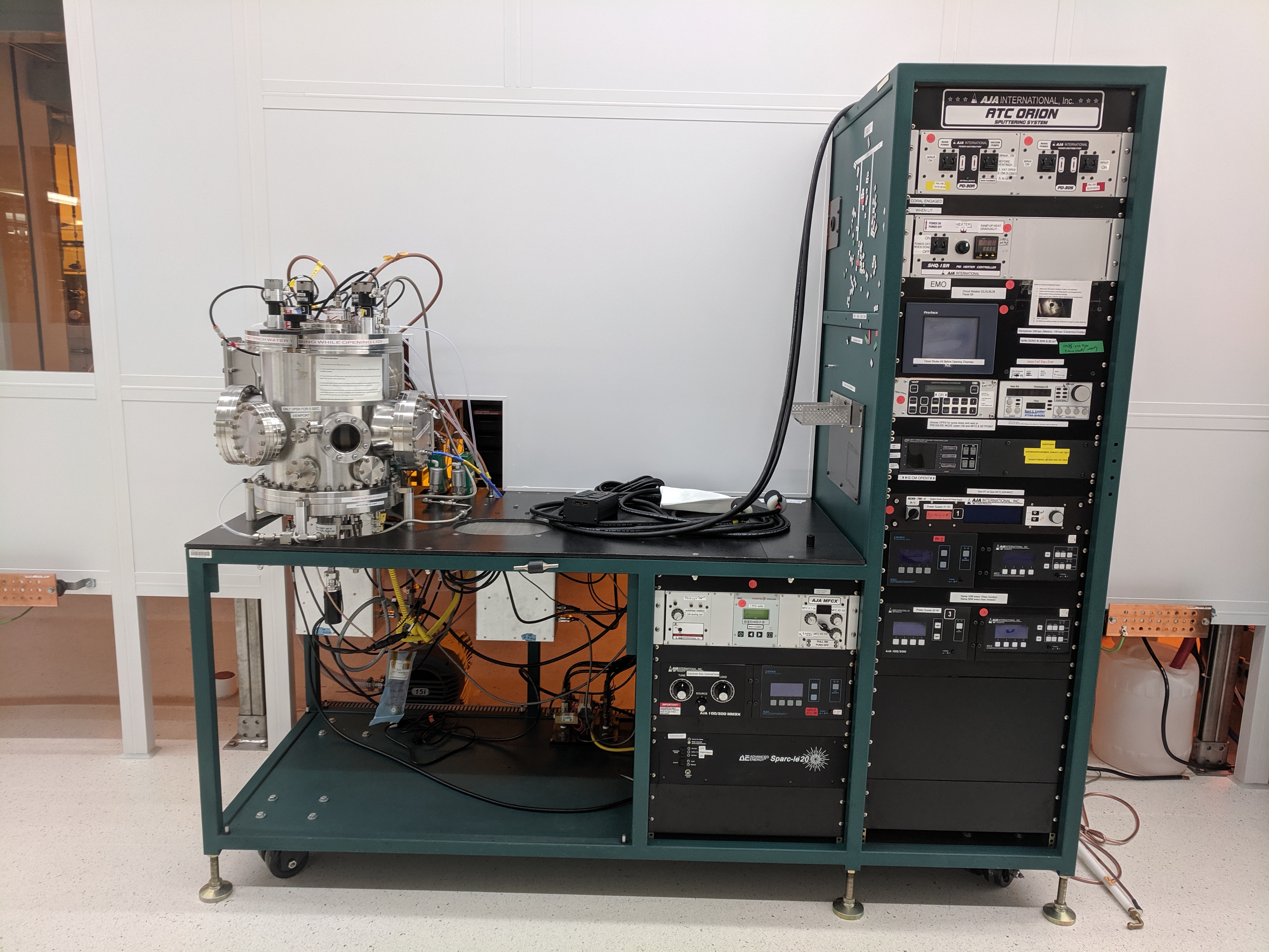
The sputterer in EML allows for the deposition of a wide variety of metals, dielectrics, and semiconductors. Reactive sputtering with O2 or N2 allows for the deposition of oxides and nitrides of these materials as well. Samples are manually loaded at the bottom of the chamber, face-up, on a rotating stage. Sputtering targets are can be changed by each user. Up to four separate targets can be loaded at a time. Up to two DC and two RF power sources are available. Substrate bias is available for etchback. Substrate heating is also available. Deposition runs of multiple metals is possible in series without the need for additional pumpdowns or venting, on wafers or pieces 3" or smaller.