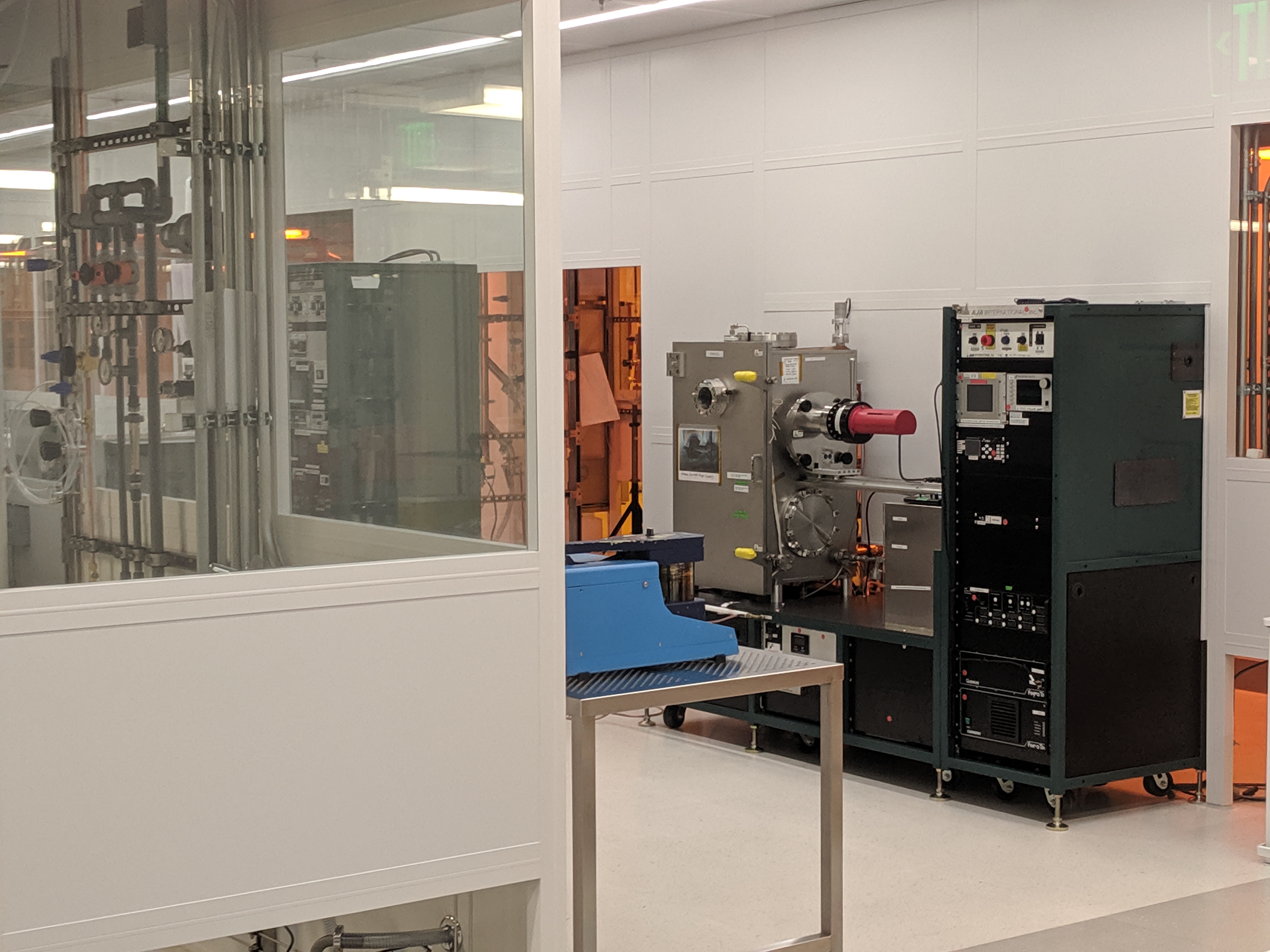
The AJA sputter tool is being moved into the MIT.nano cleanroom (behind the glass on the left), going right next to the AJA evaporator on the right.
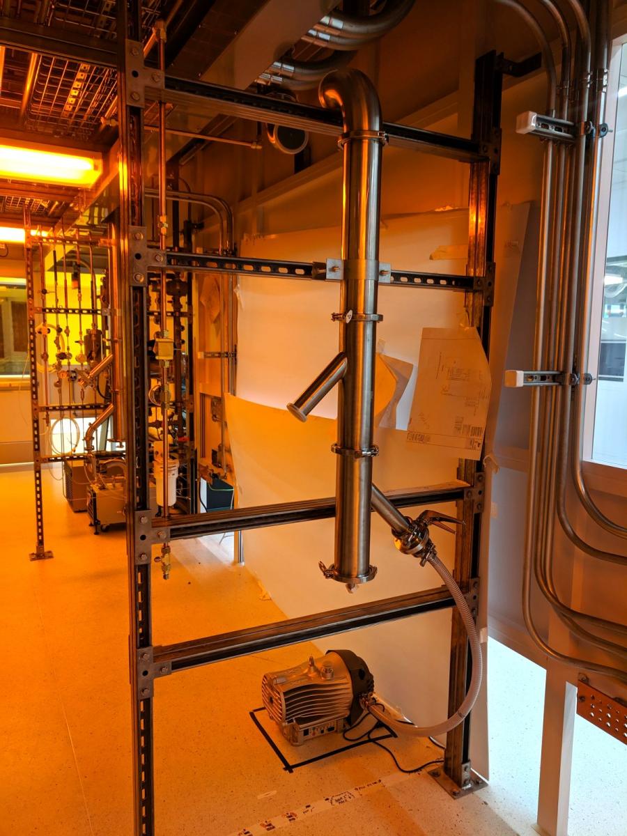
Work on the utilities was already started last month, so the wall is already cut out into the right shape and, behind the tool in the chase, power, nitrogen and water are ready to be connected to the tool. Below is a view of the inside before the tool arrives!
The sputterer in EML allows for the deposition of a wide variety of metals, dielectrics, and semiconductors. Reactive sputtering with O2 or N2 allows for the deposition of oxides and nitrides of these materials as well. Samples are manually loaded at the bottom of the chamber, face-up, on a rotating stage. Sputtering targets are can be changed by each user. Up to four separate targets can be loaded at a time. Up to two DC and two RF power sources are available. Substrate bias is available for etchback. Substrate heating is also available. Deposition runs of multiple metals is possible in series without the need for additional pumpdowns or venting, on wafers or pieces 3" or smaller.