Students in MIT's electrical engineering and computer science (EECS) course 3.155J/6.152J on micro/nano processing technology have been packaging the solar cells they fabricated at MIT.nano!
The undergraduates spent this semester designing and fabricating fluidic devices in MIT.nano's clean room. The instructors for this course are Dr. Jorg Scholvin and Dr. Jurgen Michel, and the lab instructor in the fabrication facility is Mr. Scott Poesse.
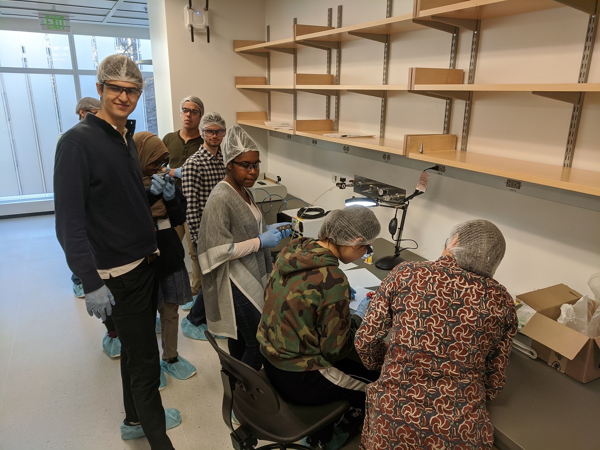
Now approaching the end of the term, the students are packaging their devices. In MIT.nano's fifth floor prototyping space, the Lab for Education and Application Prototypes (LEAP) hosts electronic and photonic packaging tools, funded by the Massachusetts Manufacturing Innovation Initiative (M2I2) of the Commonwealth of MA. Working in this space under the guidance of Dr. Agarwal, students applied a transparent epoxy using an air-powered syringe. The epoxy helps to protect the wirebonds that connect the circuit board to the solar cell.

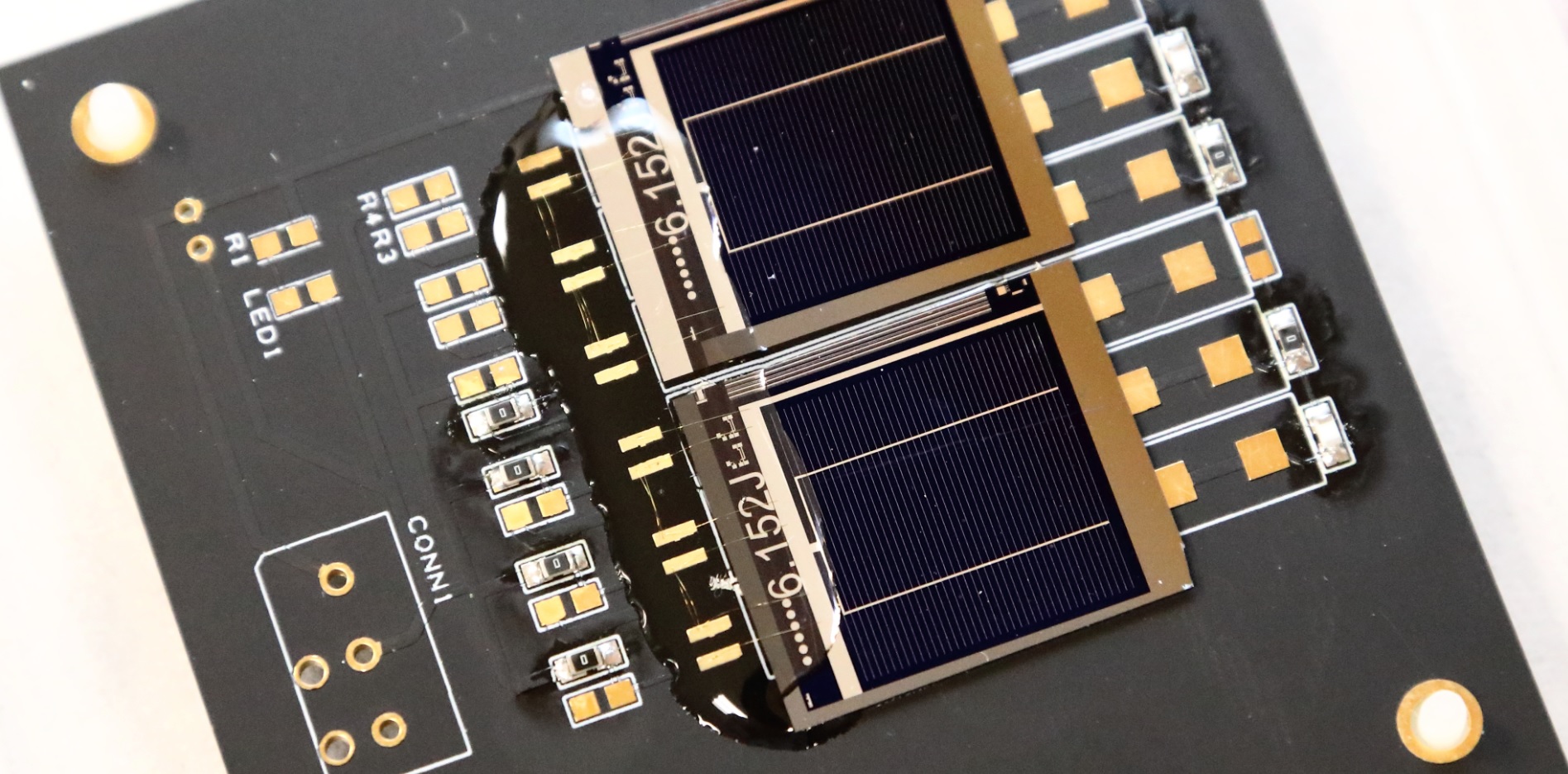
In the following figure you can see the individual wirebonds. This is a 25-micron gold wire, 1/4 of the diameter of a single strand of hair. Each cell has several wirebonds in parallel, for reliability and redundancy. However, care is taken to see that they don't excessively flex or stress the printed circuit board (PCB), to prevent breaking or detaching the wirebonds, or cleaving the solar cell from the underlying PCB.

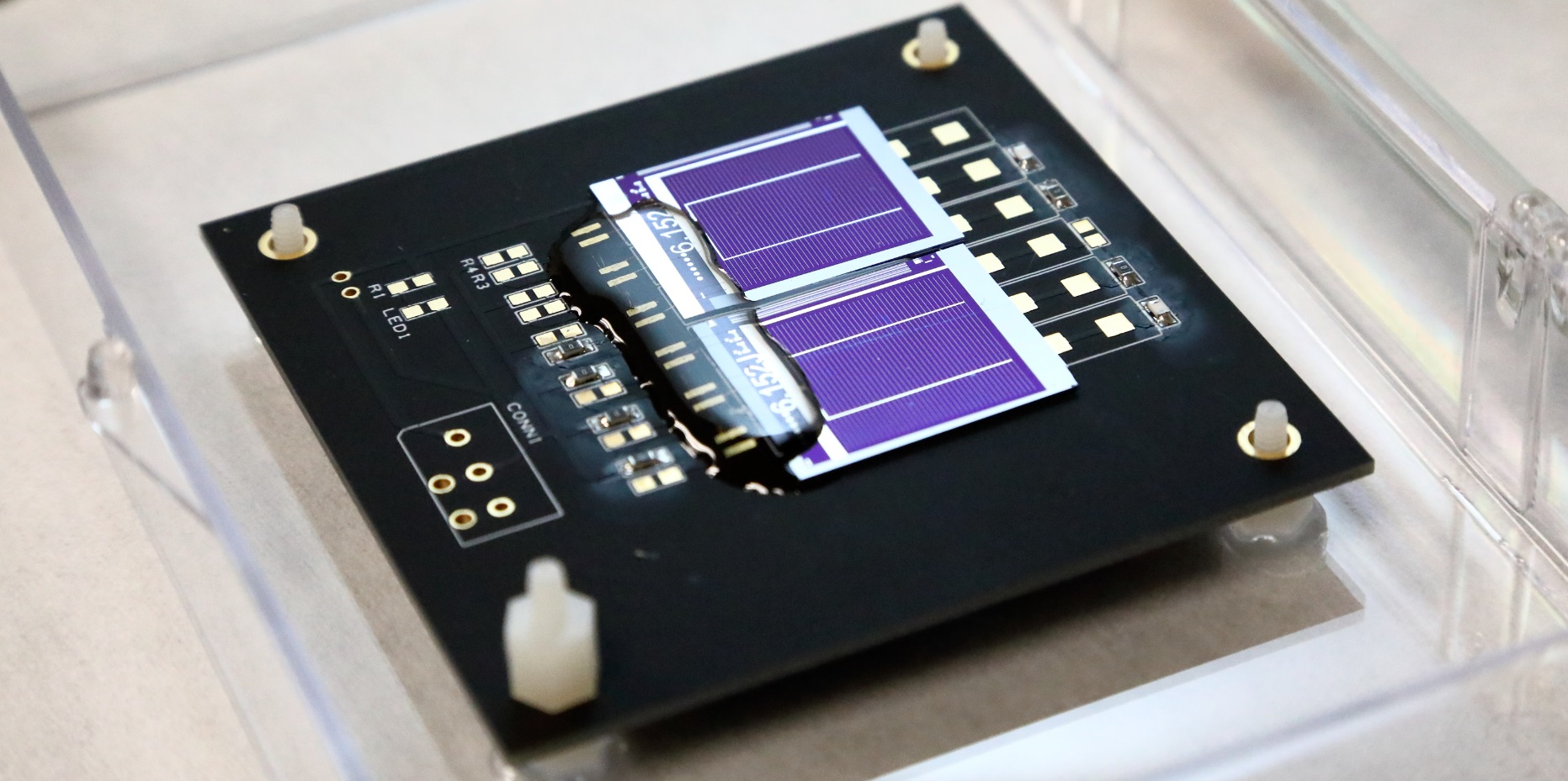
A packaged solar cell in its "travel-case" is shown below. The nylon standoff can be unscrewed to take out the cell, which is a dual-solar-cell that showed 1.05 Voc and 15 mA Isc under a white light source.

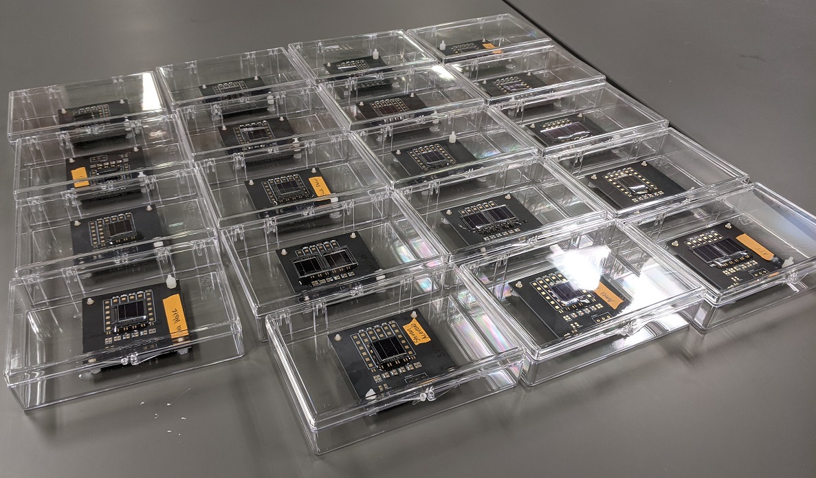
After wirebonding, but before epoxy encapsulation, students tested the devices. At the end of the day, as shown in this final image, we had a large number of packaged (and boxed) solar cells, with the epoxy curing overnight and ready to go. In this exercise, we saw 100% packaging yield, with all devices working.

