November 13, 2020
We are excited to announce that the Gemini 450 SEM, a field emission scanning electron microscope from Zeiss, is now available for training at Characterization.nano!
The instrument combines ultrahigh resolution imaging with the capability to perform advanced analytics while maintaining flexibility and ease-of-use. It is located in one of MIT.nano's basement imaging suites. Read more about the tool and sign up for training.
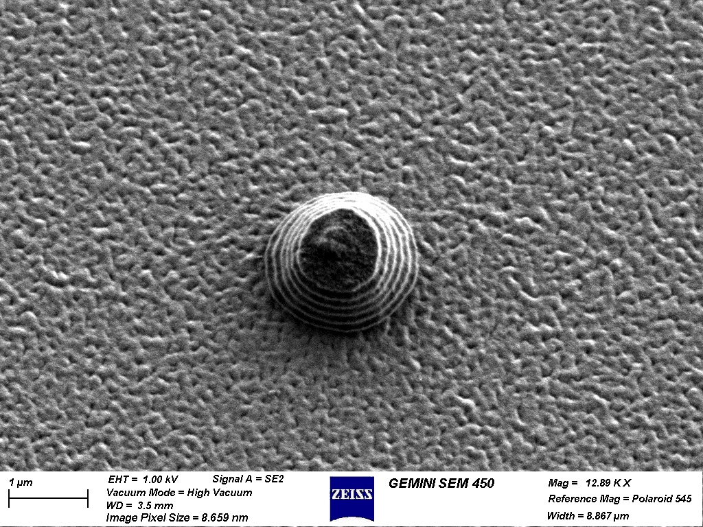
Below, you can see an example of this tool’s benefits to fab users analyzing their process. The image shows a ~1-2um circle of standard AZ3312 thin photoresist after developing (standing waves on sidewalls). Image courtesy of Benoit Desbiolles and Prof. Sarkar’s lab.