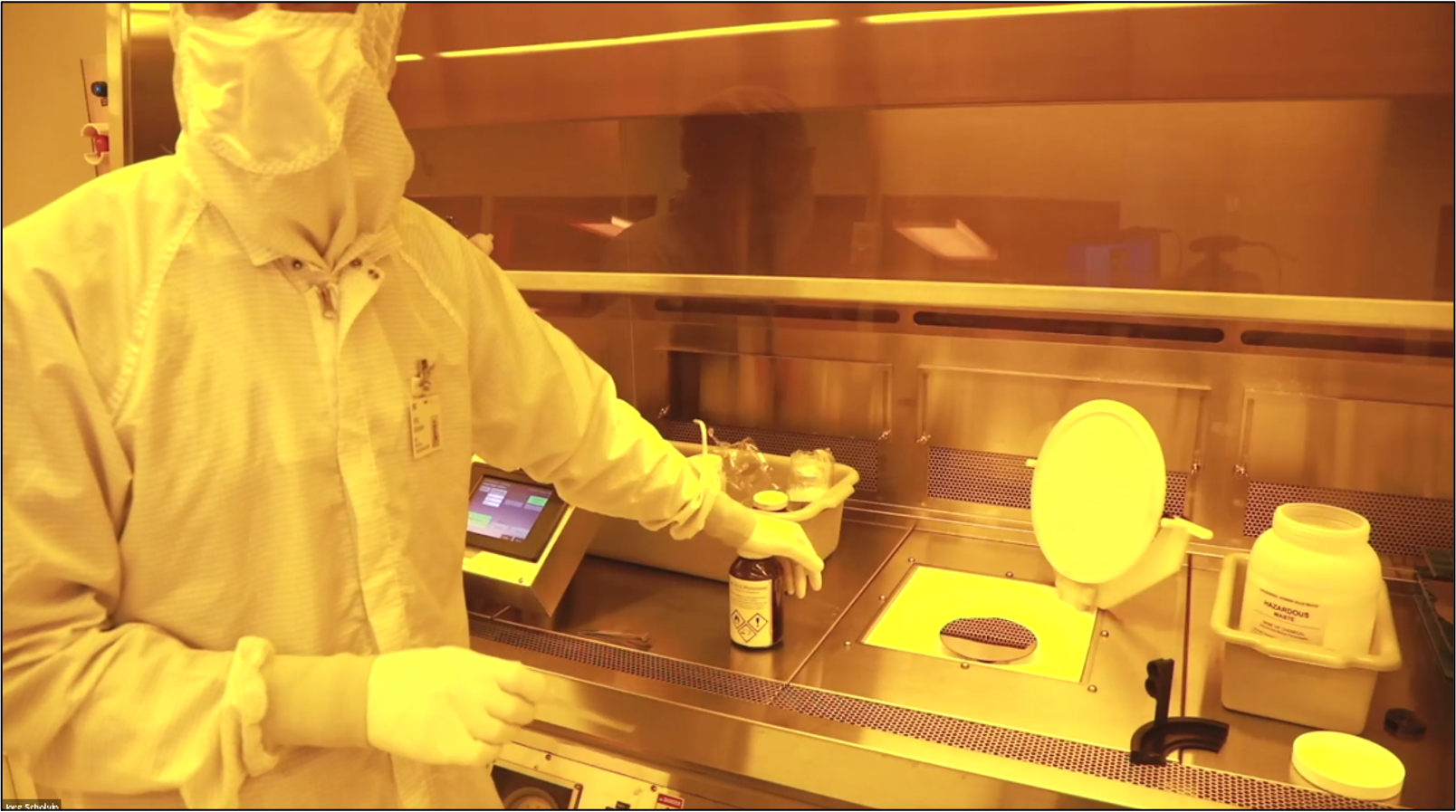
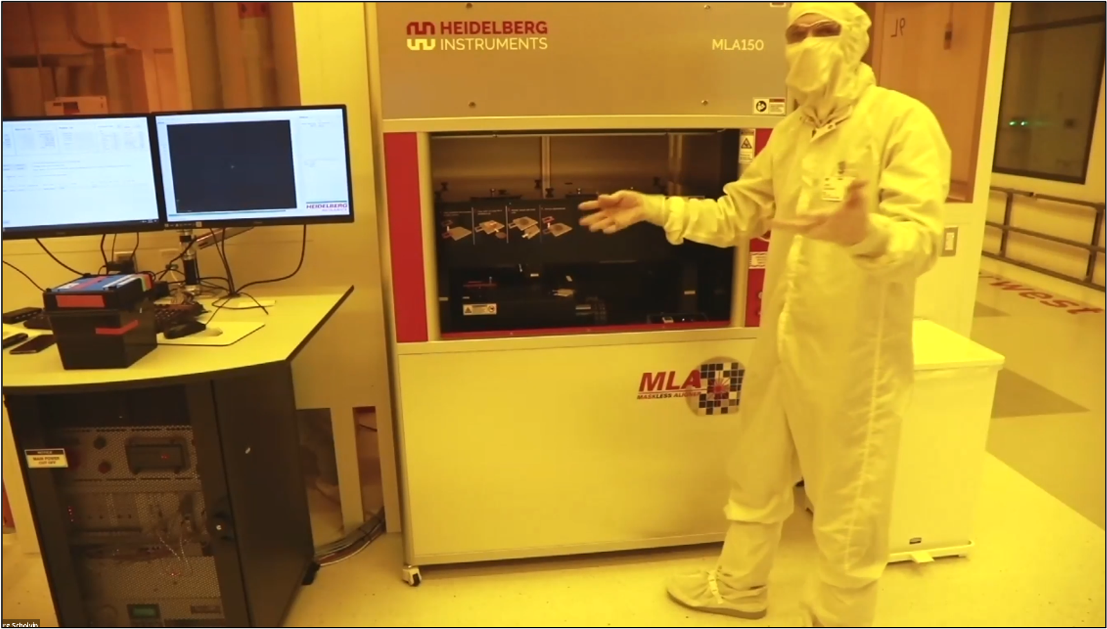
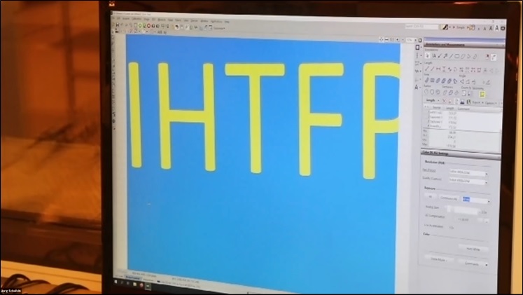
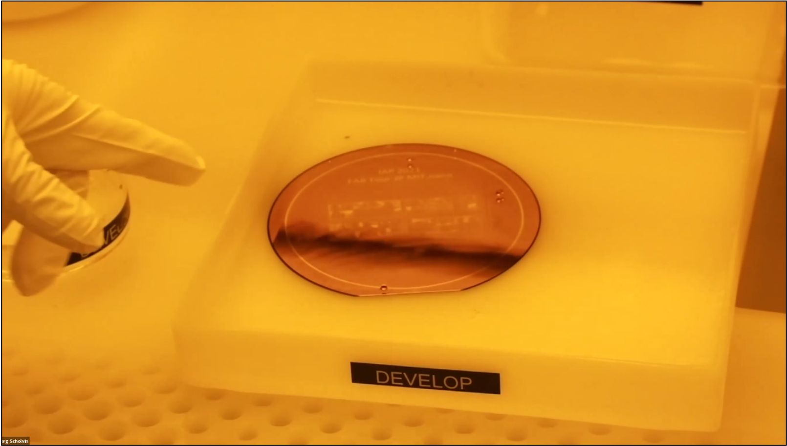
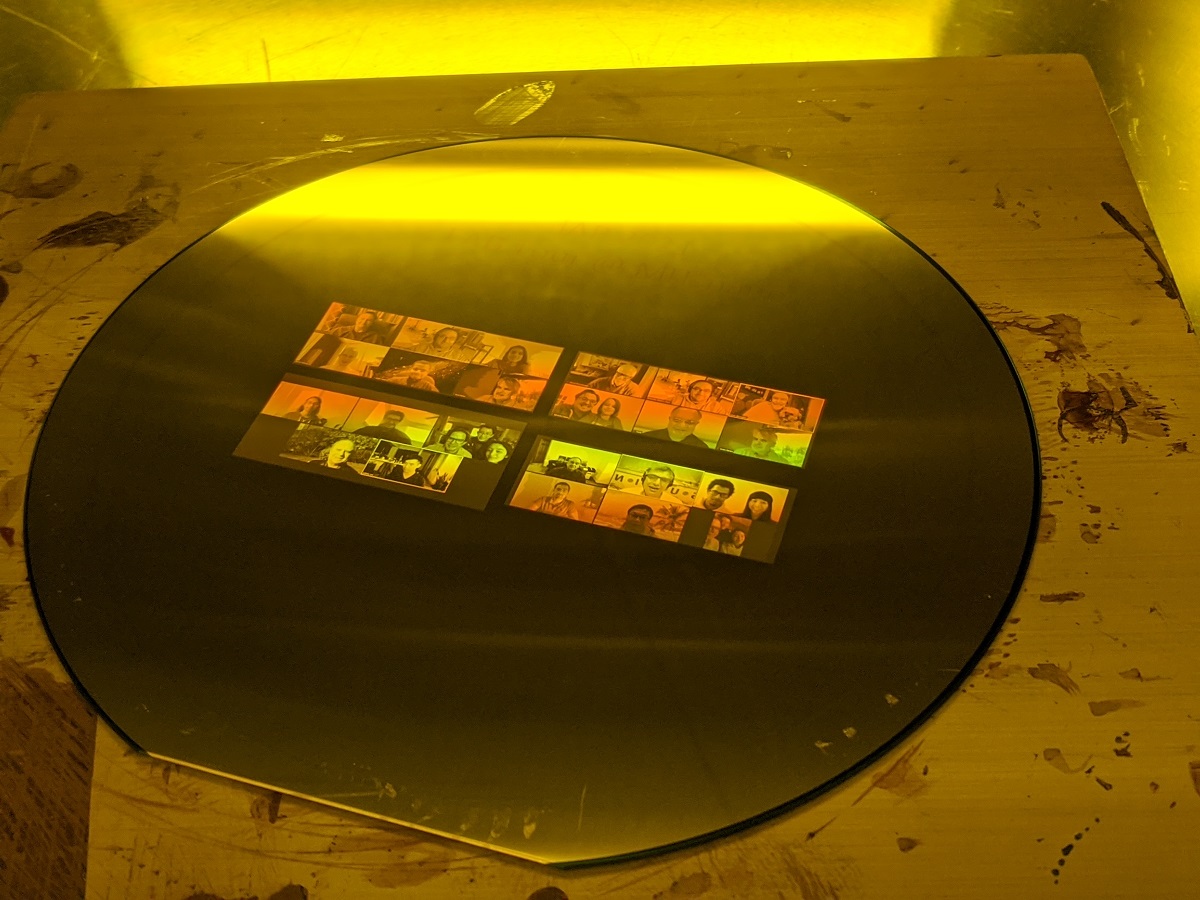
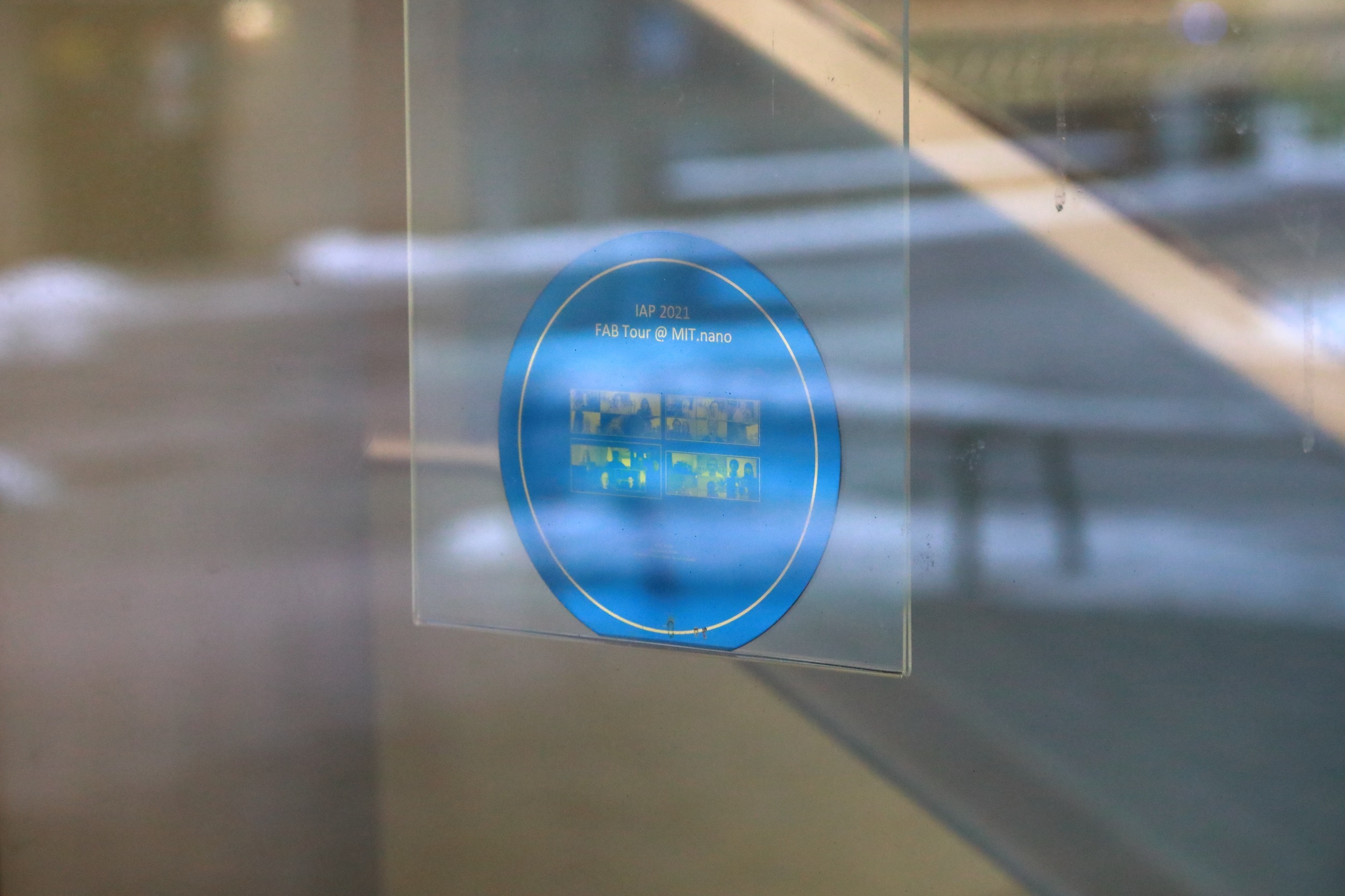
Live fabrication demo inside MIT.nano's cleanroom via Zoom.
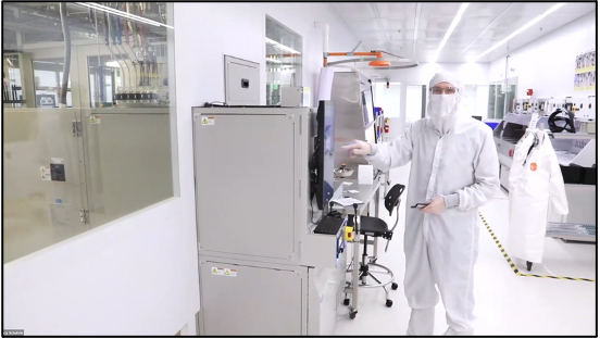
In this demonstration presented as part of MIT's Independent Activities Period (IAP), attendees learned about thin-film deposition, lithography, and etching processes at the micro- and nanoscale, as well as how to combine these techniques to build a semiconductor device. For the demo, FAB.nano Assistant Director of User Services Jorg Scholvin worked in the cleanroom to expose, develop, and etch screenshots from the Zoom workshop—and “secret” messages from the class etched in letters less than one millimeter high—onto a silicon wafer.
The wafer is now on display in the window of MIT.nano so visitors can can come by and see it (safely from outside the building) whenever they're on campus.
![Secret messages submitted by participants were etched below the images. The text is 1 mm tall.](/sites/default/files/2021-02/lg4G3A3863%20v1.jpg)
![To pattern the thin layer of gold, scientists spin-coat the wafer with photoresist. Here, the wafer is loaded onto a manual coater, and Assistant Director for User Services Jorg Scholvin is getting ready to apply the photoresist (in the bottle).](/sites/default/files/2021-03/Jorg%20creating%20wafer.png)
![Scholvin explains the operation principle of the MLA tool while the coated wafer is being exposed using a 405 nanometer blue laser.](/sites/default/files/2021-03/Jorg%20in%20front%20of%20the%20MLA.png)
![The actual gratings are shown on screen magnified 5x.](/sites/default/files/2021-02/Microscope5x.jpg)
![One of the secret messages shared by the IAP participants is shown on screen.](/sites/default/files/2021-02/VideoStill_SmallMessage.jpg)
![Once Scholvin exposed the wafer with the Zoom attendee pattern, he develops it, at which point the image is starting to appear (as the photoresist exposed by the laser is dissolved away, leaving the unexposed areas and thus creating the design).](/sites/default/files/2021-03/Wafer%20up%20close%20in%20the%20lab.png)
![The wafer after it has been developed.](/sites/default/files/2021-02/WaferAfterDevelop.jpg)
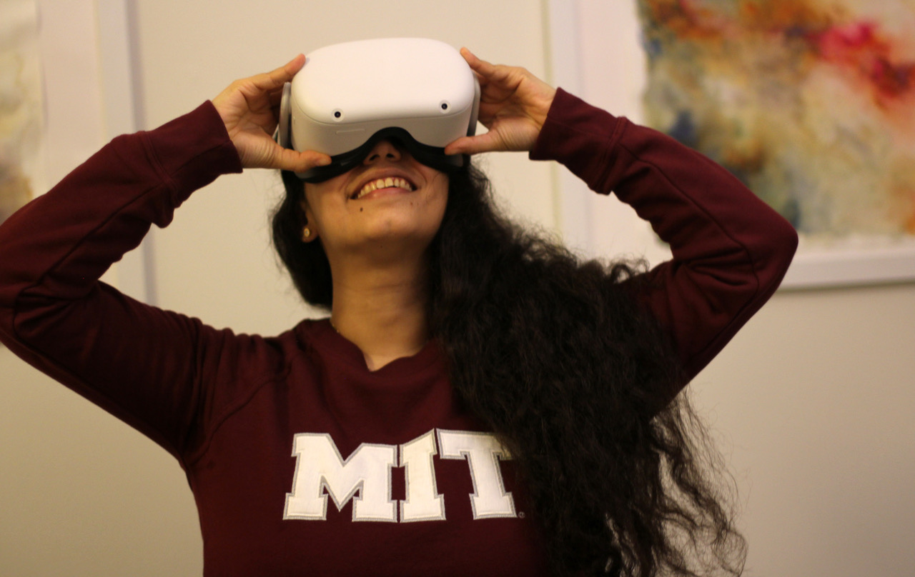
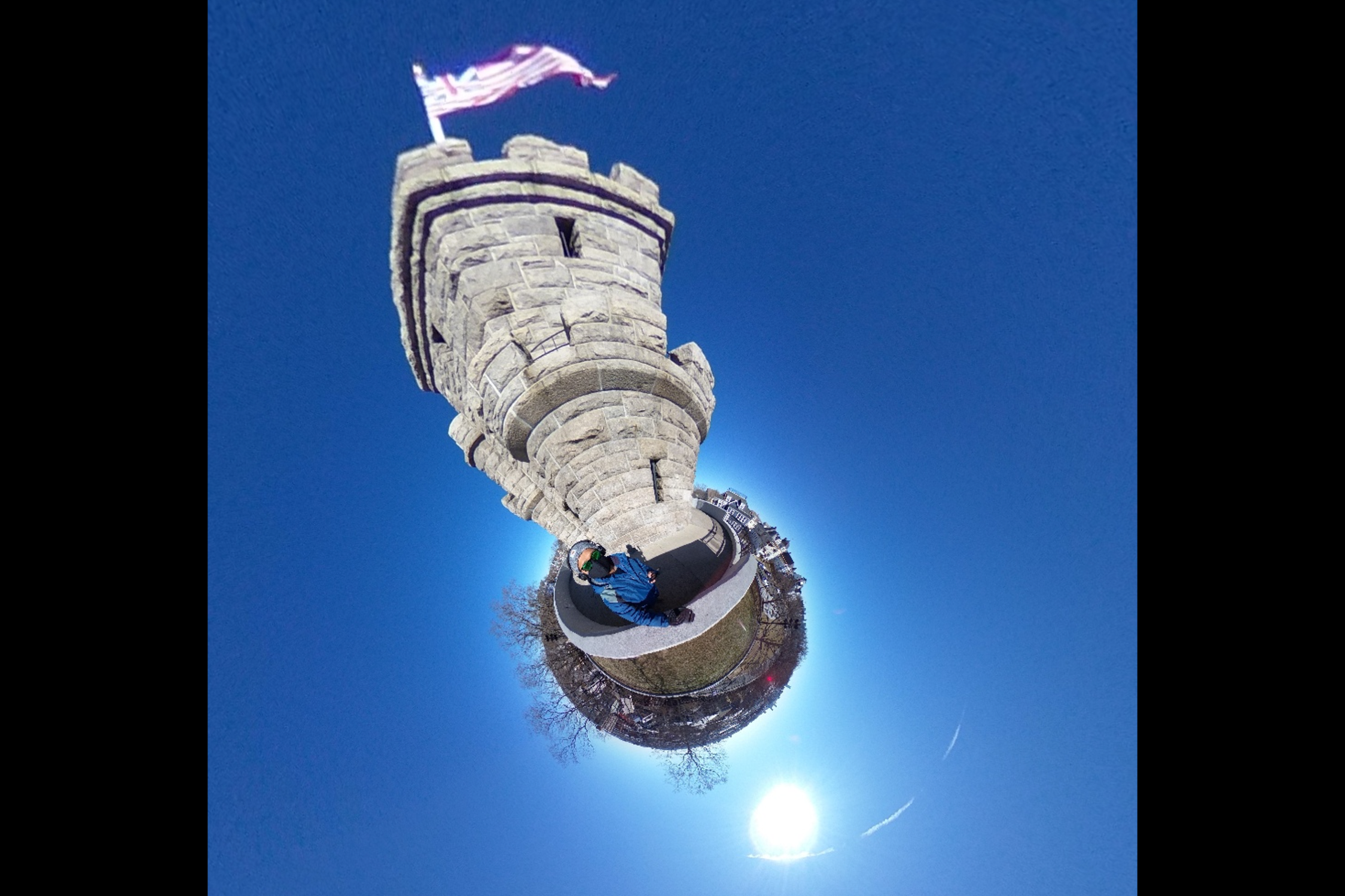
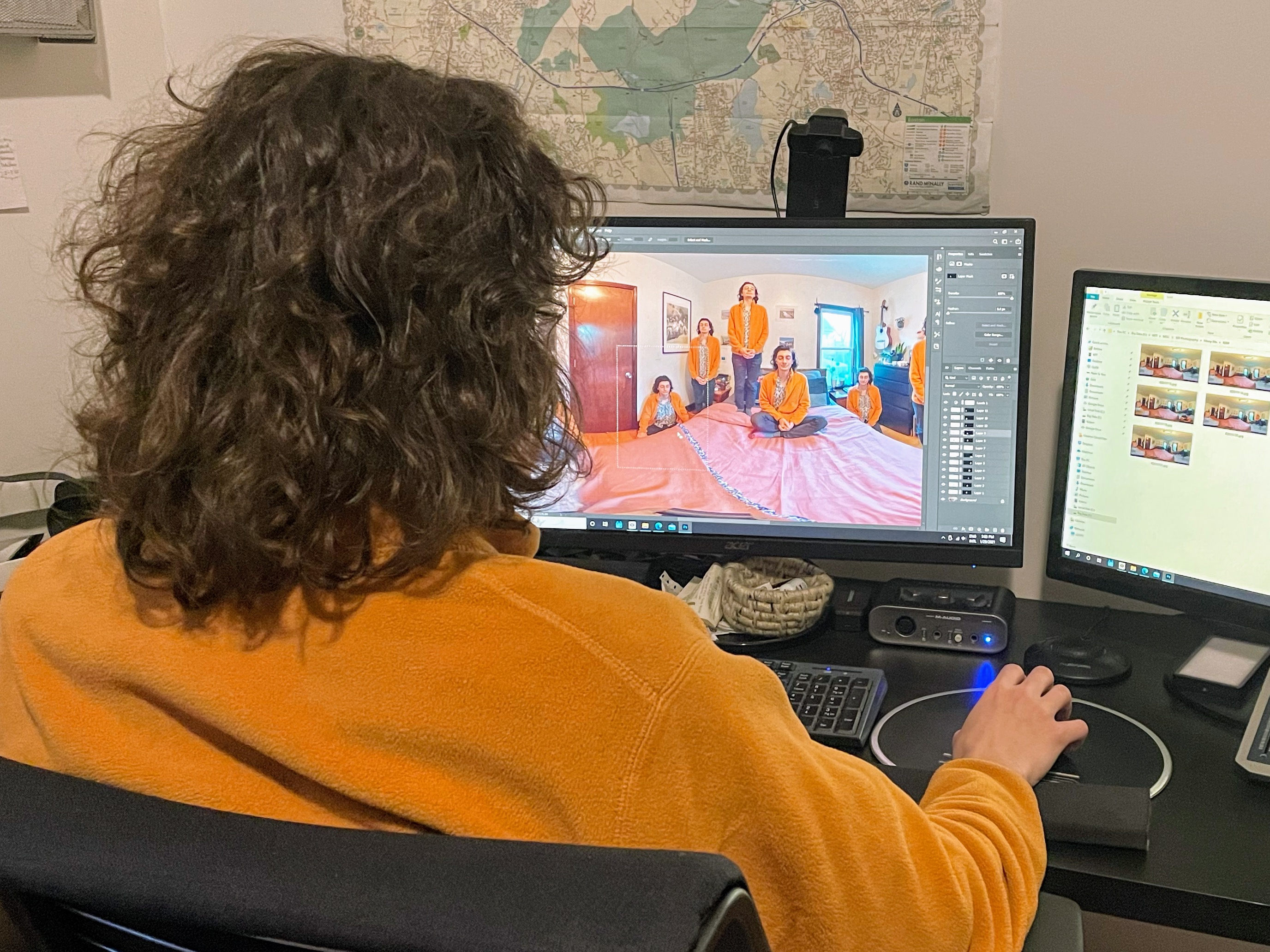
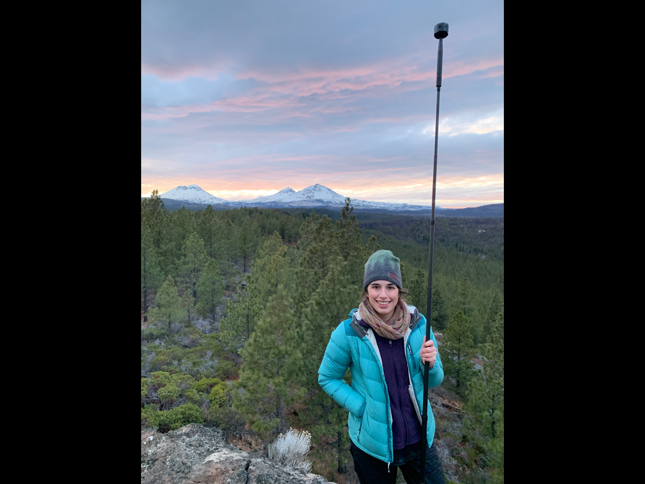
Creating, editing, and distributing 360 photography
This course, sponsored by the MIT.nano Immersion Lab and facilitated by Rus Gant, director of the Harvard Visualization Research and Teaching Laboratory, and Samantha Farrell, MIT.nano senior administrative assistant, delivered a hands-on experience to participants via Immersion Lab tools loaned to them through the mail. Students were sent a kit containing a 360 degree camera, a Quest 2 VR headset, and a monopod. Using this equipment and editing software packages, students learned to create and distribute immersive content for technical and artistic uses.
![Ambar Reyes uses an Oculus 2 headset.](/sites/default/files/2021-02/Ambar%20Reyes%20VR_1.jpeg)
![Students learn about the history of visual storytelling as part of MIT.nano's IAP course on creating, editing, and distributing 360-degree photography.](/sites/default/files/2021-02/IMG_5943.jpg)
![Students learned best practices for various methods of shooting and stabilizing their 360 cameras, followed by editing software examples, before diving in to their own projects.](/sites/default/files/2021-02/IMG_6088.jpg)
![Rohan Kundargi, Program Administrator for MIT’s Office of Government & Community Relations, uses a Ricoh Theta Z1 360 camera and monopod to practice his 360-degree photography skills at the Prospect Hill Monument in Somerville, MA.](/sites/default/files/2021-02/MIT.nano%20360%20photography%20Prospect%20Hill.png)
![Luis Zanforlin works on his video for MIT.nano's creating, editing, and distributing 360-photography course.](/sites/default/files/2021-02/Luis%20Zanforlin.jpg)
![Sarah Greer, a graduate student in mathematics, uses equipment from the MIT.nano Immersion Lab to capture 360-degree images of the mountains of Oregon.](/sites/default/files/2021-02/Sarah%20Greer%20outdoor%20360.png)
![Jorg Scholvin, Assistant Director for User Services at Fab.nano, placed a 360 camera inside the MLA-150, a direct-write laser system that can expose UV sensitive photoresist on wafers or masks, to show how the tool works.](/sites/default/files/2021-03/360-inTool.png)
![A 360-degree camera captures Jorg Scholvin, Assistant Director for User Services at Fab.nano, using the MLA from inside the tool. Scholvin uses this 360-video, created with the equipment and capabilities of the Immersion Lab, to teach new students how to use this tool in Fab.nano.](/sites/default/files/2021-03/360-inTool-2.png)
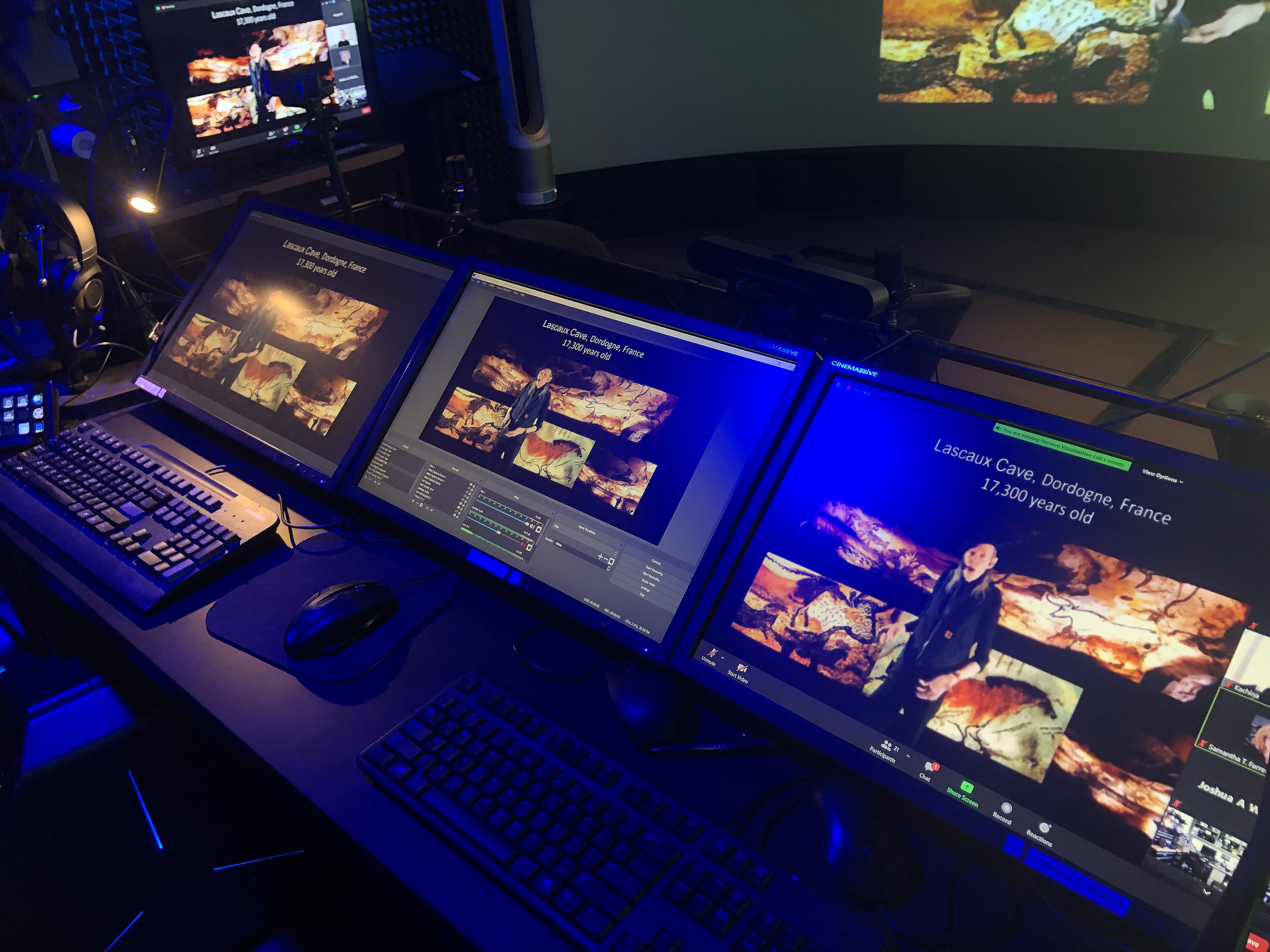
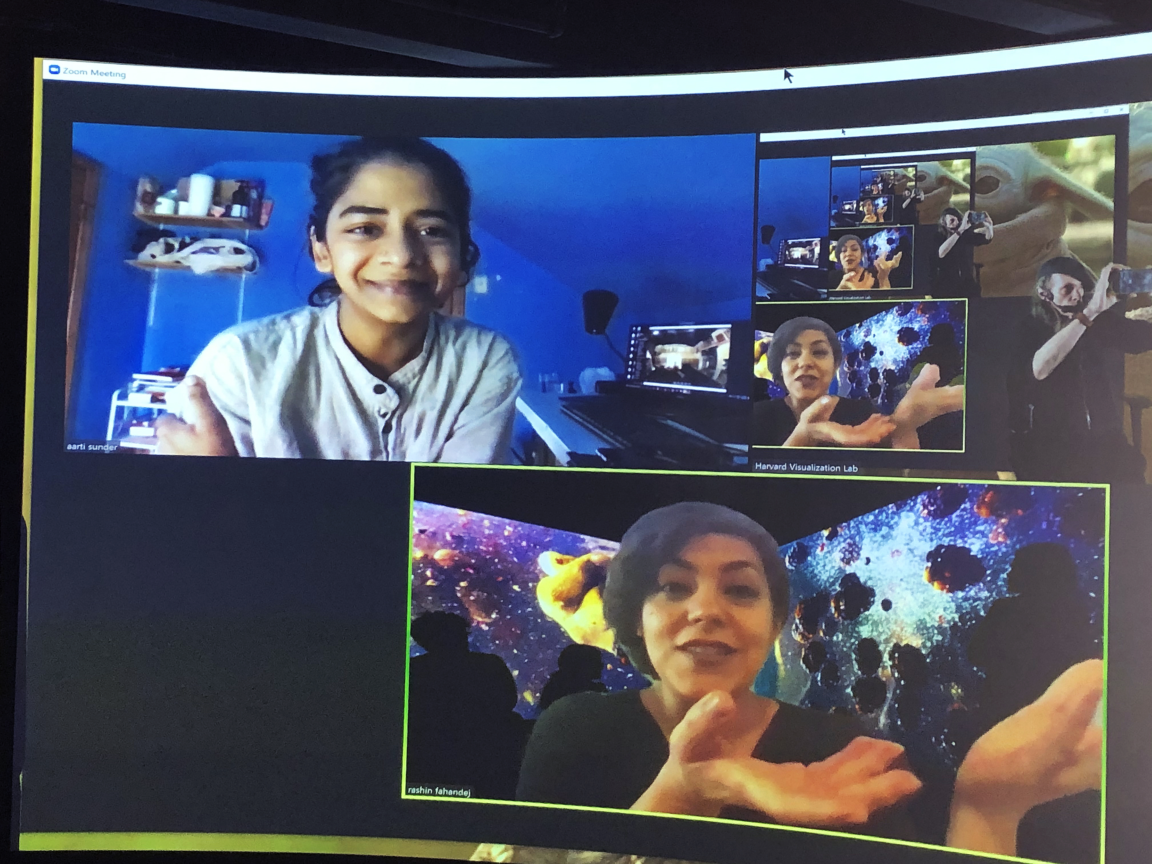
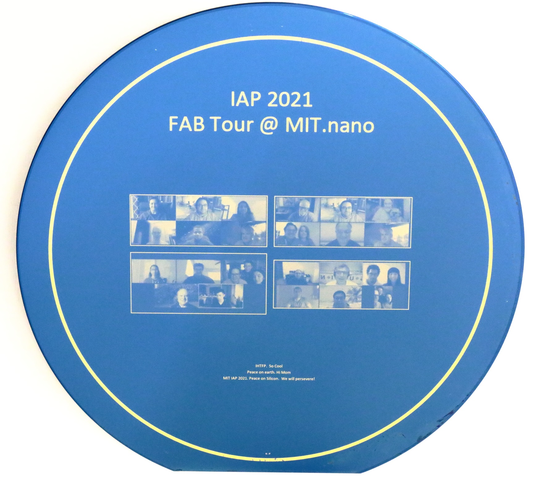
Explore MIT.nano Live
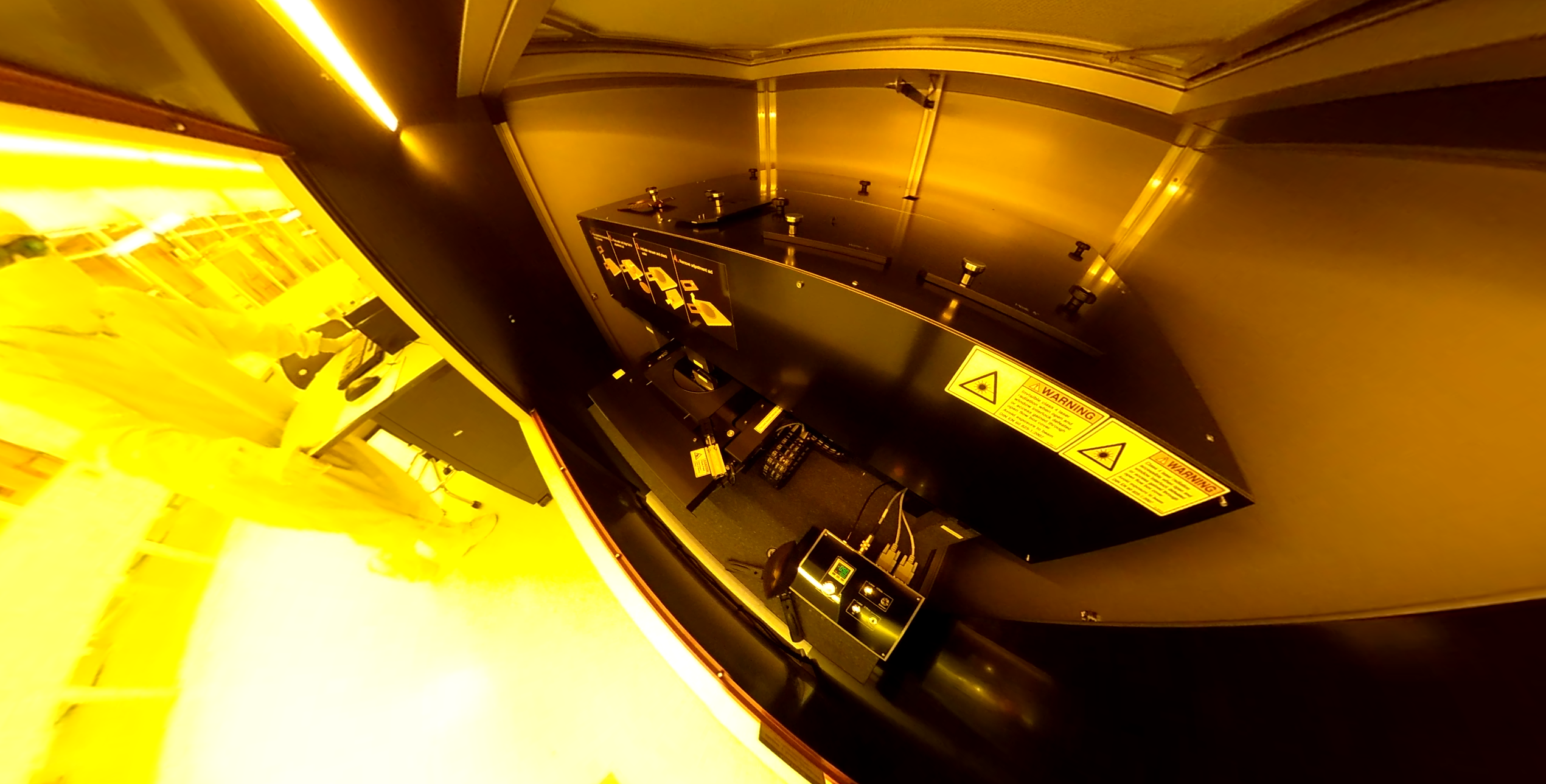
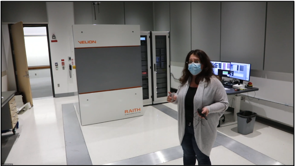
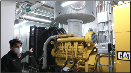
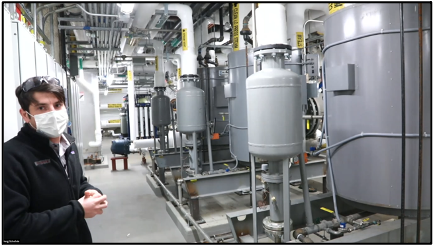
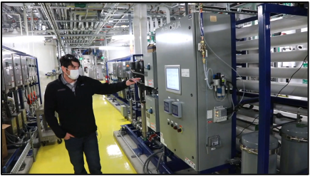
This three-part series brought participants behind the scenes of the fabrication, characterization, and supporting infrastructure at MIT.nano through virtual tours offered as part of MIT's Independent Activities Period (IAP). Attendees learned what it takes to build and see at the atomic scale, how to create a dust-free environment, how 5 million pounds of concrete helps us look at atoms, what a 1.5 Megawatt backup generator looks like, and what it takes to filter and air condition 250,000 cubic feet of fresh air every minute.
![Jorg Scholvin, assistant director for user services at Fab.nano, leads a virtual tour through MIT.nano's cleanroom.](/sites/default/files/2021-02/Fab.nano%20tour%20with%20Jorg%20Scholvin.png)
![Anna Osherov, assistant director of user services at Characterization.nano, leads a tour of the imaging suites. Here, she is telling participants about the VELION focused-ion beam scanning electron microscope.](/sites/default/files/2021-02/Characterization.nano%20tour%20with%20Anna%20Osherov.png)
![Vibrations for the MBTA red line subway are shown as part of a demonstration explaining why plinth—a 50,000-pound slab of concrete balanced on a set of springs four feet above the ground—is so important for the ultra-sensitive microscopes.](/sites/default/files/2021-02/Red%20line%20vibrations%20measured%20at%20Characterization.nano_.png)
![MIT.nano Assistant Director for Infrastructure Nick Menounos discusses MIT.nano's back-up generator.](/sites/default/files/2021-02/Infrastructure%20tour%20with%20Nick%20Menounos.png)
![Nick Menounos leads a virtual tour of MIT.nano's infrastructure.](/sites/default/files/2021-02/Infrastructure%20tour%20with%20Nick%20Menounos%202.png)
![Nick Menounos, MIT.nano's assistant director for infrastructure, leads a virtual tour of MIT.nano's non-public spaces.](/sites/default/files/2021-02/Infrastructure%20tour%20with%20Nick%20Menounos%203.png)
Biomechanics in everyday life
In this IAP course, participants learned how motion capture, photogrammetry, EMG, and virtual reality can be applied to understand more deeply how we achieve seemingly intuitive and easy tasks, and how these tools can be used in research, education, and athletic and artistic improvement. Sponsored by the MIT.nano Immersion Lab and MIT IMES Clinical Research Center (CRC), the course explored human movement through cardiovascular exercise, yoga, and meditation.
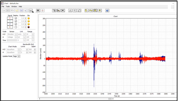
Using the MIT.nano Immersion Lab's motion capture technology and a wireless sensor system from the CRC, postdoctoral associate Praneeth Namburi shows how researchers can study physical movement of a person while jumping rope, pairing physiological measurements with exact points in the person's exercise routine.
In this next video, Namburi demonstrates the ability to track muscle length and stretching during yoga.