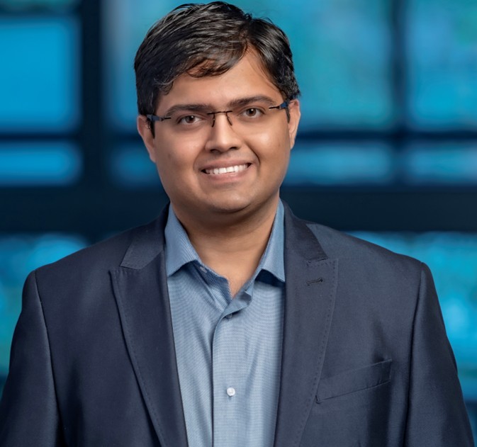
Deep Jariwala

Associate Professor and the Peter & Susanne Armstrong Distinguished Scholar
Electrical & Systems Engineering and Materials Science & Engineering
University of Pennsylvania
Date: May 5, 2025
Time: 4:00 - 5:00 PM ET
Location: Grier 34-401A
Reception to follow
ABSTRACT
Since the demise of Dennard scaling, modern computer has largely relied on architectural innovations such as multi-core processors and GPUs vs CPUs to address the evolving needs of computing paradigm. This problem has been exacerbated since computing has largely evolved from arithmetic centric to data centric in the age of billions of internet-connected devices and artificial intelligence. Thus, dense and reliable data storage combined with fast and high bandwidth access in novel memory devices has become the frontier for research in modern computing hardware.
There have been several advancements across a variety of technologies in the past three decades. Ferroelectric materials and devices are among the forefront of these technologies due to their low-power and fast switching abilities, but suffer from integration challenges. Simultaneously, developing data-heavy computing architectures in extreme environments is a growing need and a frontier challenge since silicon carbide (SiC), which is the leading logic technology for elevated temperature environments, is limited by computing power and lack of memory devices that can operate at elevated temperatures.
In this talk, Jariwala will make the case of how novel III-nitride materials might present interesting avenues to overcome some of the above limitations being faced by both silicon and silicon carbide (SiC) hardware. He will present ongoing and recent work on integration of 2D chalcogenide semiconductors emerging wurtzite structure ferroelectric nitride materials[1] namely aluminum scandium nitride (AlScN).
First, Jariwala will present on Ferroelectric Field Effect Transistors (FE-FETs) made from 2D materials when integrated with AlScN and make the case for 2D semiconductors in this application.[2-4] He will then show recent results on scaling 2D/AlScN FE-FETs, achieving ultra-high carrier and current densities[5] in ferroelectrically gated MoS2 and also demonstrate negative-capacitance FETs[6] by engineering the AlScN/dielectric/2D interface.
Then, Jariwala will introduce the ferroelectric diode (FeD) memory device[7] and demonstrate multi-bit operation[8] as well as compute in memory (CIM)[9] using FeD devices made from AlScN. Finally, he will demonstrate why AlScN FeDs are uniquely suited as a high temperature non-volatile memory demonstrating stable operation up to 600 C[10] and how AlScN can be integrated onto SiC[11] for stable data retention in ferroelectric capacitors up to 800 C.[12] He will end by providing a broad outlook on both AI computing hardware as well as high-temperature computing.[13]
References:
[1] Kim, K.-H.;et al. Jariwala, D. Nature Nanotechnology 2023, 18 (5), 422-441..
[2] Liu, X.; et al. Jariwala, D. Nano Letters 2021, 21 (9), 3753-3761.
[3] Kim, K.-H.; et al. Jariwala, D. Nature Nanotechnology 2023, 18, 1044–1050.
[4] Kim, K.-H.; et al. Jariwala, D. ACS Nano 2024, 18 (5), 4180-4188.
[5] Song, S.; et al. Jariwala, D. ACS Nano 2025.
[6] Song, S.; et al. Jariwala, D. Applied Physics Letters 2023, 123 (18).
[7] Liu, X.; et al. Jariwala, D. Applied Physics Letters 2021, 118 (20), 202901.
[8] Kim, K.-H.;et al. Jariwala, D. ACS Nano 2024, 18 (24), 15925-15934.
[9] Liu, X.; et al. Jariwala, D. Nano Letters 2022, 22 (18), 7690–7698.
[10] Pradhan, D. K.; et al. Jariwala, D. Nature Electronics 2024, 7 (5), 348-355.
[11] He, Y.; et al. Jariwala, D. Applied Physics Letters 2023, 123 (12).
[12] He, Y.; et al. Jariwala, D. Nano Letters 2025.
[13] Pradhan, D. K.; et al. Jariwala, D. Nature Reviews Materials 2024, 9 (11), 790-807.
Watch the webcast
Ask your questions
BIOGRAPHY
Deep Jariwala is an associate professor and the Peter & Susanne Armstrong Distinguished Scholar in the Electrical and Systems Engineering as well as Materials Science and Engineering at the University of Pennsylvania (Penn). Jariwala completed his undergraduate degree in metallurgical engineering from the Indian Institute of Technology in Varanasi and his Ph.D. in materials science and engineering at Northwestern University. Jariwala was a Resnick Prize Postdoctoral Fellow at Caltech before joining Penn to start his own research group. His research interests broadly lie at the intersection of new materials, surface science and solid-state devices for computing, opto-electronics and energy harvesting applications in addition to the development of correlated and functional imaging techniques.
Jariwala’s research has been widely recognized with several awards from professional societies, funding bodies, industries as well as private foundations, the most notable ones being the Optica Adolph Lomb Medal, the Bell Labs Prize, the AVS Peter Mark Memorial Award, IEEE Photonics Society Young Investigator Award, IEEE Nanotechnology Council Young Investigator Award, IUPAP Early Career Scientist Prize in Semiconductors, the SPIE Early career achievement award and the Alfred P. Sloan Fellowship. He has published over 150 journal papers with more than 22000 citations and holds several patents. He serves as the Associate Editor for ACS Nano Letters and has been appointed as a Distinguished Lecturer for the IEEE Nanotechnology Council for 2025.
