Advancements in electrical and optical characterization technologies
12-0168, MIT.nano (basement level), Building 12
60 Vassar Street (rear)
Cambridge, MA
An advanced suite of electrical and optical characterization solutions is a key component of the research and development for semiconductor, photovoltaic and photonics devices where a detailed understanding of the electronic behavior of materials is essential.
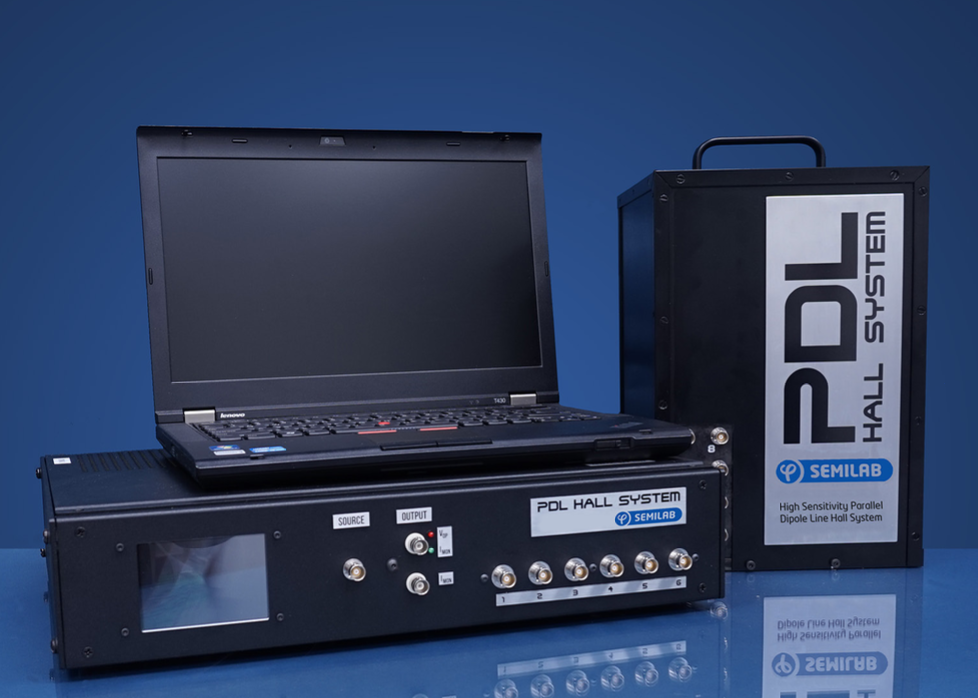
In this talk, Semilab experts will review spectroscopic ellipsometry solutions via variety of application examples from different research areas including semiconductor, photonics and pharmaceuticals as well as present a new compact AC Hall effect measurement technique using a unique Parallel Dipole Line (PDL) configuration allowing measurements of VDP Hall mobilities down to 0.1cm^2/V-s without the need for large electromagnets and water cooling. During the tech talk, the basics of VDP Hall Measurements will be explained, along with a live demonstration of the equipment in a variety of potential applications.