The Independent Activities Period (IAP) is a special term at MIT that runs from early January until the end of the month. IAP provides members of the MIT community (students, faculty, staff, and alums) with a unique opportunity to organize, sponsor and participate in a wide variety of activities, including how-to sessions, forums, athletic endeavors, lecture series, films, tours, recitals and contests.
MIT.nano is offering the following courses during IAP 2024:
Make your own chip inside the lab!
 Instructor: Jorg Scholvin, Associate Director Fab.nano
Dates & times (participants will be assigned one session):
(additional dates added on 1/17)
Tuesday, 1/9, 2pm - 5pm
Wednesday, 1/10, 2pm - 5pm
Thursday, 1/11, 9am - 12pm
Monday, 1/15, 2pm - 5pm
Wednesday, 1/17, 9am - 12pm
Thursday, 1/18, 2pm - 5pm
Friday, 1/19, 2pm - 5pm
Saturday, 1/20, 2pm - 5pm (new)
Thursday, 1/25, 2pm - 5pm
Friday, 1/26, 2pm - 5pm
Friday, 1/26, 6pm - 9pm (new)
Tuesday, 1/30, 9am - 12pm
Tuesday, 1/30, 2pm - 5pm
Wednesday, 1/31, 2pm - 5pm
Thursday, 2/1, 9am - 12pm
Friday, 2/2, 2pm - 5pm
Friday, 2/2, 6pm - 9pm (new)
Location: MIT.nano cleanroom (12-3001)
Register here - rolling registration based on availability
Step inside MIT.nano’s fab to create a 1x1 inch chip with your favorite image to take home with you! We will work inside the MIT.nano cleanroom: learn how to gown up, understand the different fab tools, and use the tools to pattern a 50 nm thin layer of aluminum with your design. At the end, we will separate out the chips from the wafer, and you get a chance to put your chip in a small frame or carrier to take with you.
Each session is limited to 12 students. On the registration form, please indicate at which sessions you would be available. We will begin communicating assigned dates and times on January 2, 2024.
Into the Structure-Verse: An introduction to crystallographic structure determination with x-rays and electrons
 Instructors: Aubrey Penn, Research Specialist; Jordan Cox, Research Specialist
Date: Wednesday, January 17, and Thursday, January 18, 2024
Time: 9:00 AM – 1:00 PM
Location: MIT.nano conference room 12-5001 (new location)
Registration closed - course is full
Limited to 10 participants. This is a two-day course—participants must attend both days.
This course is designed to introduce attendees to best practices in crystallographic structure determination with x-rays and electrons. Attendees will learn about XRD, electron diffraction, and scanning transmission electron microscopy on crystalline materials, with a primary focus on data analysis. A hands-on lab will be offered for XRD structure model refinement as well as an introduction to image analysis with the python package Atomap.
Previous python experience is not required, but attendees will find introductory experience helpful. It is encouraged that attendees download anaconda before the course begins. This will be a 2-day course: one day for X-rays and one day for electrons. We welcome students who may not have formal education in crystallography, XRD and/or TEM.
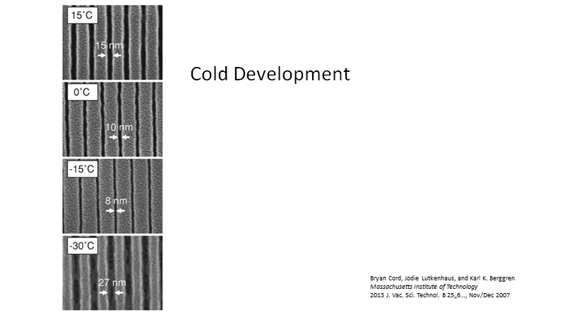
A brief introduction to e-beam lithography
 Instructors: Mark Mondol, Assistant Director Nano Structures Laboratory; and Juan Ferrera, Research Scientist
Date: Thursday, January 18, 2024
Time: 1:00 PM – 2:30 PM
Location: MIT.nano Building 12 Room 0168 (Basement teaching space)
Registration is now closed
Limited to 40 participants.
E-beam lithography enables advanced semiconductor chips; without e-beam lithography minimum features sizes would be limited to approximately 200 nm. In research environments, e-beam lithography allows direct write, maskless lithography enabling quick and relatively cheap design changes.
This talk introduces the basics of e-beam lithography and pattern transfer, including electron energy, material interaction, limits to resolution, e-beam resists, throughput, proximity effect correction, and characteristics of different e-beam lithography tools.
Anyone with an interest in e-beam lithography, from neophyte, to experienced user should be able to gain something from this talk.
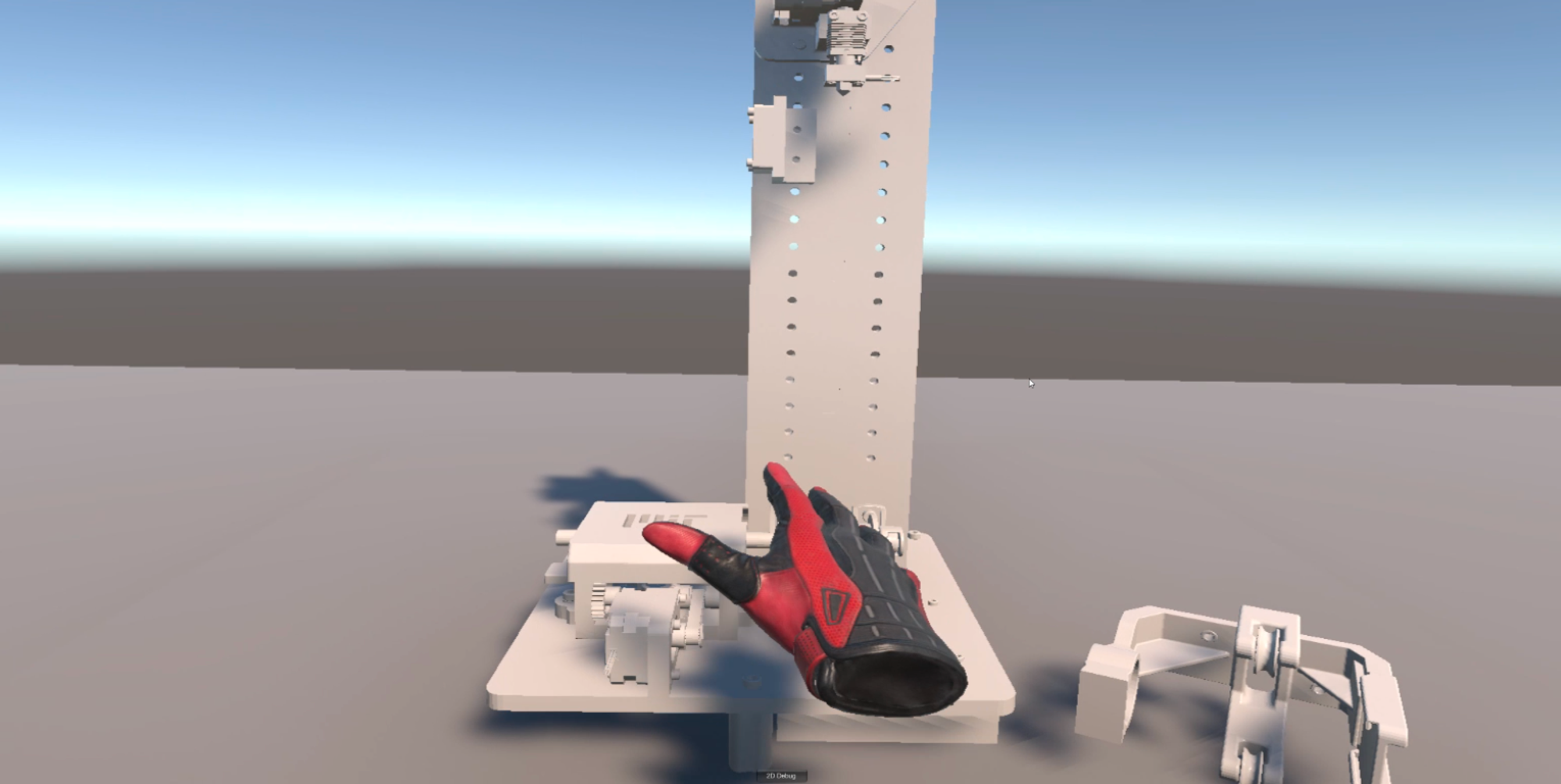
How to think like a VR developer
 Instructors: Talis Reks, AR/VR/Gaming/Big Data IT Technologist; Y. Jenny Wang, Lecturer, XR developer, researcher, and consultant
Dates & times:
Tuesday, January 30, 2024, 10am - 12pm
Wednesday, January 31, 2024, 10am - 12pm; 1pm - 4pm
Friday, February 2, 2024, 1pm - 3pm
Location: MIT.nano Immersion Lab (12-3207)
Registration is now closed
Limited to 15 individuals. Participants must attend all sessions.
This is a beginner’s hands-on guide for getting started in VR/AR development. We will introduce the fundamentals of working in virtual reality, explain the basic pipeline, and provide support for you to complete a project. This workshop is designed to give you hands-on experience working with a game engine (Unity) and iterative design of VR/AR experiences. No prior experience with VR or coding is required.