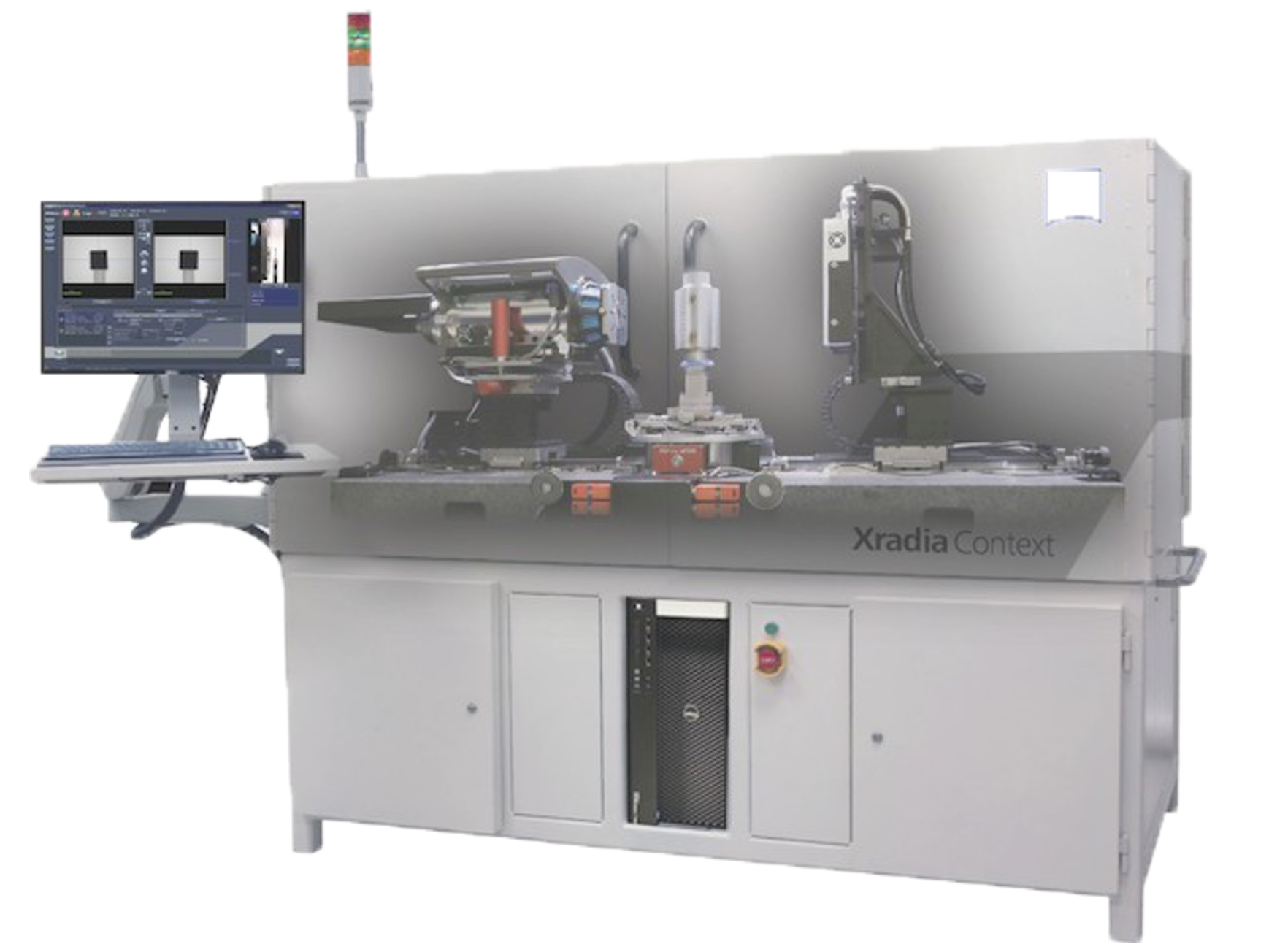
The pharmaceutical industry is under growing pressure from patent expirations of major drugs, cost-constrained health care systems, and a demanding regulatory environment. A focus for the industry is to tackle these challenges while increasing the output and quality of cost-effective, new medicines without incurring unsustainable R&D cost. Through new technology and new approaches there is an aspiration to make such improvements while also bringing ever-improved therapeutics to patients faster.
In this conference, we will lay out many of the challenges the industry is facing and explore potential solutions coming from academic research and startup endeavors, from early discovery through manufacturing technologies, to clinical studies and beyond.
9 a.m. – 5 p.m. EDT
Read more and register.